Citi Bank has published a research report on AI-PCB, indicating that with the GB200 and GB300 combined with ASICs experiencing explosive growth, and the upgrade of switches from 800G to 1.6T, AI-PCB is expected to see over 50% growth in 2026. Due to the sudden surge in demand, the industry capacity was fully loaded by Q1 2025, and new capacity will take 18-24 months to build, resulting in a 10% capacity gap.The entire sector has shown a trend of diffusion from the perspective of the market, from PCBs to upstream CCLs, then to electronic fabrics, transitioning from ordinary materials to upgraded special materials. Today, I will provide a deep analysis of this. The production chain of PCBs basically revolves around “Substrate -> Copper Clad Laminate (CCL) -> PCB”: 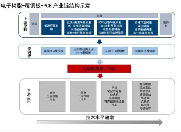 1. PCBThe direct material for manufacturing PCBs is CCL. The manufacturing process for high-end PCBs is still quite complex, and here, equipment is key. Currently, the market has not yet tapped into the equipment sector, so I will list a table:
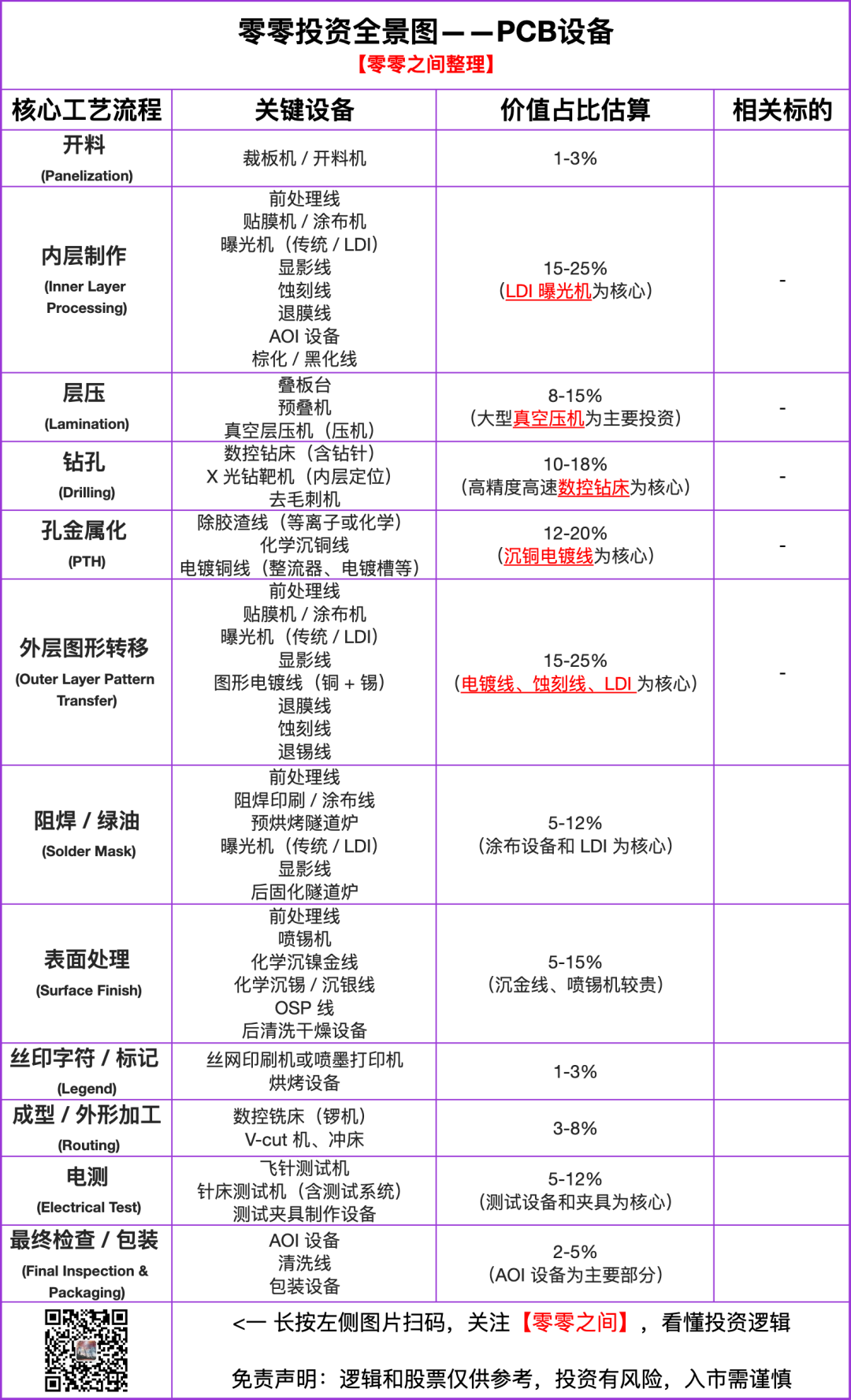 2. CCLCCL has different grades. Ordinary PCBs have lower requirements for CCL. In the AI field, servers, switches, and optical modules following GB200 require CCL of M8 grade or higher. Taking NVIDIA as an example, whether for servers, switches, or optical modules, they all use high-level HDI, and the specific requirements for CCL are detailed in the table:
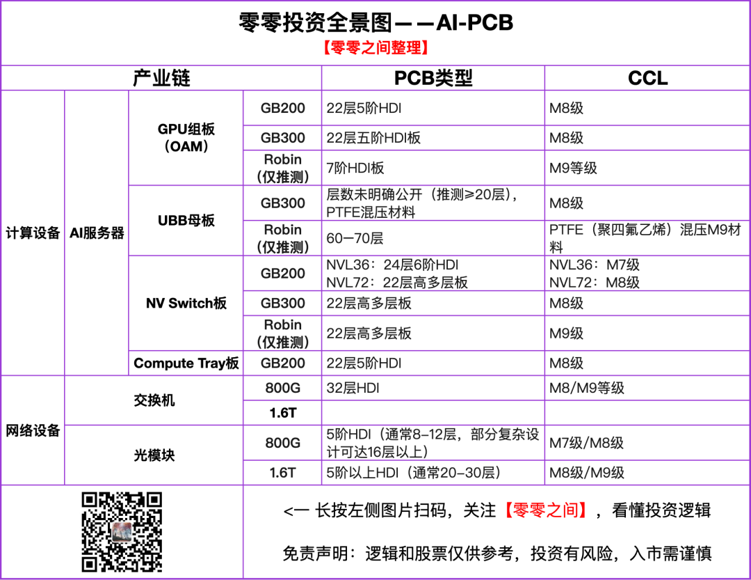 To manufacture CCL, it typically involves plating a layer of copper on the substrate. For M8 and M9 grade CCL, in addition to substrate requirements, the copper itself must have a very smooth surface. Currently, the mainstream copper foil is still third generation, with the fourth generation rapidly growing, while the fifth generation is still under development, and leading companies in Japan and South Korea have yet to ship, although two companies in China have advantages.3. Substrate The substrate usually involves the electronic fabric (also known as glass fiber fabric, quartz fabric) and resin being precisely compounded.Electronic Fabric: The current mainstream is still the first generation, which occupies about 80% of the current market share, dominated by two major suppliers in Japan, leaving us with little room to enter. However, with the explosion of 800G and 1.6T optical modules, to meet M8 grade requirements, the second generation of electronic fabric must be used, and currently, the supply of the second generation is severely insufficient. Japan and Taiwan Glass have weak expansion intentions, providing us with a significant opportunity to enter, as several domestic capacities are about to be established. Subsequently, the emergence of Rubin will necessitate the third generation of electronic fabric.Resin: Currently, epoxy resin is predominant, and similarly, with the iteration of chips, the resin has evolved from epoxy to modified, and then to PTFE, with the next generationRubin being essential.The above outlines the main content of AI-PCB, emphasizing that AI-PCB primarily refers to circuit board PCBs, not IC substrates, as these are not the same concept.The overall situation is complex, and I hope everyone will communicate and share more. Thank you for your support!~More opportunities await in the community