Capacitors play a crucial role in high-speed PCB design and are typically the most used components on a PCB. In PCBs, capacitors are generally categorized into filtering capacitors, decoupling capacitors, and energy storage capacitors.
1. Power Output Capacitors, Filtering Capacitors
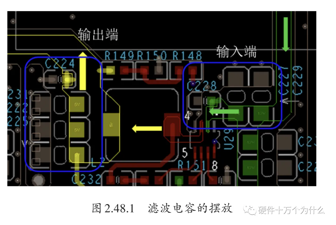
The capacitors in the input and output circuits of the power module are commonly referred to as filtering capacitors. Simply put, these capacitors ensure the stability of the input and output power. In power modules, the principle for placing filtering capacitors is “larger first, smaller later.” As shown in Figure 2.48.1, the filtering capacitors are arranged in the direction of the arrow from larger to smaller.
During power design, it is important to ensure that the traces and copper areas are sufficiently wide and that there are enough vias to meet the current carrying capacity requirements. The width and number of vias should be evaluated based on the current size.
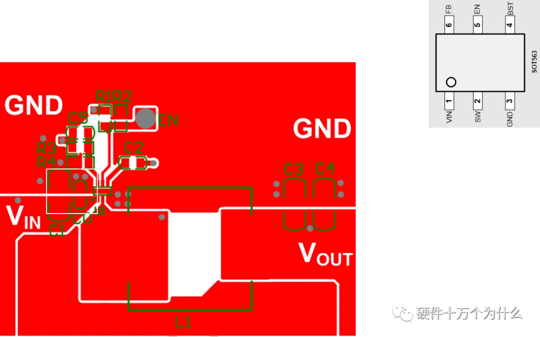
Power Input Capacitors
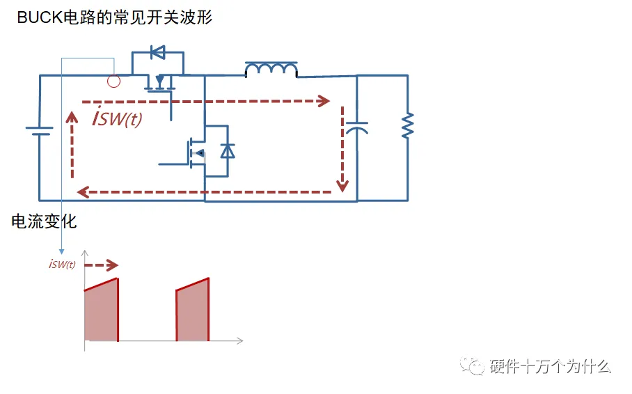
The power input capacitor forms a current loop with the switching loop. The variation in this current loop is significant, with the amplitude of Iout. The frequency corresponds to the switching frequency. During the switching process of the DC-DC chip, the current change generated by this current loop includes a rapid di/dt.
In synchronous BUCK configurations, the current path must pass through the chip’s GND pin, and the input capacitor should be connected between the chip’s GND and Vin, with the path kept as short and wide as possible.
A smaller area for this current loop will improve its radiation characteristics.
2. Decoupling Capacitors
High-speed IC power pins require a sufficient number of decoupling capacitors, ideally one for each pin. In practical designs, if there is insufficient space for decoupling capacitors, they can be reduced as necessary.
The capacitance values for decoupling capacitors on IC power pins are typically small, such as 0.1μF or 0.01μF; the corresponding packages are also small, like 0402 or 0603. When placing decoupling capacitors, the following points should be noted:
(1) Place them as close to the power pins as possible; otherwise, they may not effectively decouple. Theoretically, capacitors have a certain decoupling radius, so the proximity principle should be strictly followed.
(2) The leads from the decoupling capacitors to the power pins should be as short as possible and should be thickened, typically with a width of 8 to 15 mils (1 mil = 0.0254 mm). The purpose of thickening is to reduce lead inductance and ensure power performance.
(3) After the leads from the decoupling capacitor’s power and ground pins exit the pads, they should be connected to the power and ground planes via nearby vias. These leads should also be thickened, and larger vias should be used whenever possible; if a 10 mil via can be used, do not use an 8 mil via.
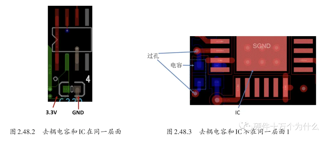
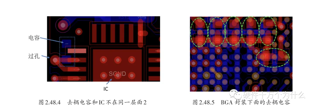
(4) Ensure that the decoupling loop is as small as possible. Common placement examples for decoupling capacitors are shown in Figures 2.48.2 to 2.48.4. The placement methods for SOP package IC decoupling capacitors are similar to those for QFP packages.
In common BGA packages, decoupling capacitors are usually placed underneath the BGA, on the back side. Due to the high pin density of BGA packages, decoupling capacitors are generally not placed in large numbers, but efforts should be made to place as many as possible, as shown in Figure 2.48.5.
3. Energy Storage Capacitors
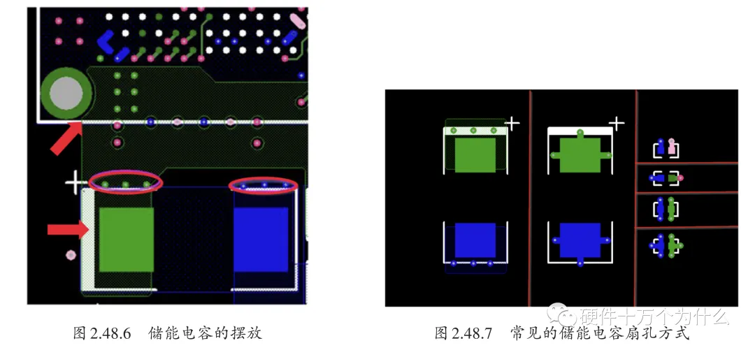
The role of energy storage capacitors is to ensure that the IC can provide electrical energy in the shortest time when in use. The capacitance values for energy storage capacitors are generally larger, and the corresponding packages are also larger. In PCBs, energy storage capacitors can be placed further away from the components, but not too far, as shown in Figure 2.48.6. Common fan-out methods for energy storage capacitors are illustrated in Figure 2.48.7.
The principles for fan-out and fan-in of capacitors are as follows:
(1) Keep leads as short and thick as possible to minimize parasitic inductance.
(2) For energy storage capacitors or devices with large current, multiple vias should be used as much as possible.
(3) Of course, the best electrical performance for fan-out is through-hole vias. Practical considerations must be taken into account.

[1]Driven by Interest and Passion
[2] Should Hardware Engineers Design Their Own PCBs?
[3]How Long Should PCB Traces Be??
[4]How Wide Should PCB Traces Be?
[5]What Are the Internal Layers of a PCB?
[6]Vias
[7]Can PCBs Have Sharp Angles and Right Angles?
[8] Should Dead Copper Be Retained? (PCB Islands)
[9]Can Vias Be Placed on Pads??
[10] PCB Materials, What Does FR4 Refer To?
[11] Solder Mask, Why Is Green Oil Mostly Green?
[12]Steel Mesh
[13]Pre-layout
[14]Key Points for PCB Layout and Routing
[15] Cross-segment Routing
[16] Signal Reflection
[17] Dirty Signals
[18] Surface Treatment Processes Such as Gold Plating, Gold Coating, and Tin Spraying
[19] Line Spacing
[20] Placement of Capacitors
[21] Crosstalk
[22] Flying Probe Testing of PCBs
[23] Overview and Simulation of FPC
[24] Why Do PCBs Deform and Bend? How to Solve It?
[25] Understanding “Characteristic Impedance” in One Article
[26] Layer Design of PCBs
[27] Reflow Paths for High-Speed Circuit PCBs
[28] Power Handling and Plane Segmentation in PCB Design
[29] Zigzag PCB Routing – Tabbed Routing
[30] What Is the Dielectric Loss Angle in PCBs?
[31] The Impact of Copper Foil Roughness on High-Speed Signals
[32] Why Should Crystals Not Be Placed at the Edges of PCBs?
[33] What Are High-Speed Signals?
[34] What Is a Transmission Line?
[35] Pre-emphasis, De-emphasis, and Equalization
[36] How to Utilize PCB Heat Dissipation
[37] “Stub” in PCB Design
[38] Dilemma: Should There Be a GND Protection Line Between Traces?
[39] PCB Copper Pour
[40] Rules to Follow When Designing PCBs
[41]“Pseudo Eight Layers” in PCB Layer Design
[42] Besides Stripline and Microstrip, There Is Also “Co-planar Waveguide”
Parameters Related to PCB Pad Design
Why Should Ground Holes Be Drilled at the Edges of PCBs?
PCBs That Are Easier to Dissipate Heat: Aluminum Substrates
[46] Why Should Reference Planes Be Hollowed Out?
Crystal Oscillator PCB Design
Designing PCB for DC/DC Power Supplies with EMC Considerations
PCB Turns, Round Corners Are Not Always the Best Routing
Why Should Vias Be Sealed? “Conductive Via Plugging Process”
Key Points for Power PCB Layout and Routing
Mark Points on PCB
Simulating High-Speed Signals Across Segments Using ADS
Rigid-Flex Boards (Soft-Hard Combined Boards)
Mixed Signal PCB Design