
1. PCB Current and Trace Width
The calculation of PCB current-carrying capacity has long lacked authoritative technical methods and formulas. Experienced CAD engineers can make relatively accurate judgments based on personal experience. However, for new CAD users, this can be quite a challenge.
The current-carrying capacity of a PCB depends on the following factors: trace width, trace thickness (copper foil thickness), and allowable temperature rise. It is well known that the wider the PCB trace, the greater the current-carrying capacity.
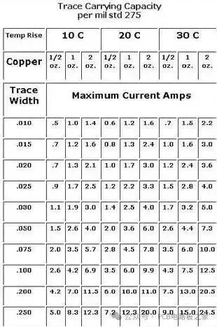
Assuming under the same conditions, if a 10MIL trace can carry 1A, how much current can a 50MIL trace carry? Is it 5A? The answer is naturally no. Please see the data provided by an international authoritative organization below:
● The unit of trace width is: Inch (1 inch = 2.54 cm = 25.4 mm)
● Data: MIL-STD-275 Printed Wiring for Electronic Equipment
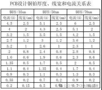
2. The Relationship Between PCB Design Copper Thickness, Trace Width, and Current
Before understanding the relationship between PCB design copper thickness, trace width, and current, let us first understand the conversion between the unit of copper thickness in PCB design, which is often expressed in ounces, inches, and millimeters: “In many data sheets, the copper thickness of PCBs is often expressed in ounces, and the conversion relationship with inches and millimeters is as follows:
1 ounce = 0.0014 inches = 0.0356 millimeters (mm)
2 ounces = 0.0028 inches = 0.0712 millimeters (mm)
Ounces are a unit of weight, and the reason it can be converted to millimeters is that the copper thickness of the PCB is ounces per square inch.
Table of the Relationship Between PCB Design Copper Thickness, Trace Width, and Current:
An empirical formula can also be used for calculations:
0.15 × Trace Width (W) = A, where the above data is the current-carrying capacity of the trace at a temperature of 25°C.
Wire impedance: 0.0005 × L/W (length/width)
Additionally, the current-carrying capacity of the wire is related to the number of vias and pads.
The current-carrying capacity of the wire is directly related to the number of vias and pads (currently, no calculation formula has been found for the impact of pad and via diameter per square millimeter on the current-carrying capacity of the trace). Here, we will briefly discuss some of the main factors affecting the current-carrying capacity of the trace.
1. The current-carrying values listed in the table are the maximum current-carrying values at a normal temperature of 25 degrees, so various environmental factors, manufacturing processes, board material processes, and board quality must also be considered in actual design. Therefore, the table provides only a reference value.
2. In actual design, each trace will also be affected by pads and vias. For example, if a segment of a trace has too many pads, after soldering, the current-carrying capacity of that segment will greatly increase. Many people have seen segments of traces burned out between pads on high-current boards.
The reason is simple: after soldering, the pads, due to the component leads and solder, enhance the current-carrying capacity of that segment of the trace, while the maximum current-carrying capacity between pads is limited to the maximum current-carrying capacity allowed by the trace width.
Therefore, during instantaneous fluctuations in the circuit, it is very easy to burn out the segment of the trace between pads. The solution is to increase the trace width. If the board does not allow for an increase in trace width, an additional solder layer can be added (generally, a 1mm trace can have an additional solder layer of about 0.6, or you can add a 1mm solder layer trace). This way, after soldering, this 1mm trace can be considered as a 1.5mm to 2mm trace (depending on the uniformity and amount of solder during soldering), as shown in the figure below:
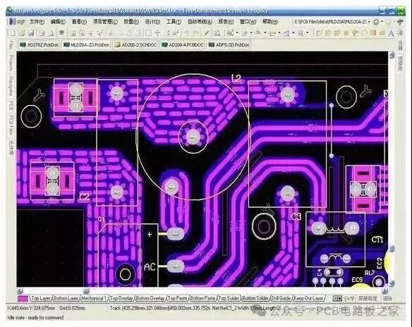
This type of processing method is familiar to those engaged in small appliance PCB layout. Therefore, if the soldering amount is uniform and sufficient, this 1mm trace can be considered as more than a 2mm trace, which is particularly important in single-sided high-current boards.
3. The processing method around the pads in the figure is also to increase the uniformity of the current-carrying capacity between the trace and the pads, which is particularly important in boards with large current thick leads (where the lead is greater than 1.2 and the pad is greater than 3).
Because if the pad is greater than 3mm and the lead is greater than 1.2, after soldering, the current of that pad will increase by several times. If a large current fluctuation occurs, the current-carrying capacity of the entire trace will become very uneven (especially when there are many pads), making it very likely to cause the trace between pads to burn out.
The processing method shown in the figure can effectively distribute the uniformity of the current-carrying capacity between a single pad and the surrounding traces.
Finally, it is reiterated: the current-carrying capacity data table is only an absolute reference value. When not designing for high currents, adding 10% to the values provided in the table will definitely meet design requirements.
In general single-sided board design, with a copper thickness of 35um, it can be designed at a 1:1 ratio, meaning that 1A of current can be designed with a 1mm trace, which will meet the requirements (calculated at a temperature of 105 degrees).
3. The Relationship Between Copper Foil Thickness, Trace Width, and Current in PCB Design
The strength of the signal current. When the average current of the signal is large, the current that the trace width can carry should be considered, and the trace width can refer to the following data.
The relationship between copper foil thickness, trace width, and current in PCB design, the current-carrying capacity of copper foils of different thicknesses and widths is shown in the table below:
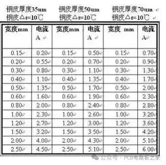
Note:
i. When using copper foil as a wire to carry large currents, the current-carrying capacity of the copper foil width should be selected considering a derating of 50% based on the values in the table.
ii. In PCB design and processing, ounces (OZ) are commonly used as the unit of copper thickness, where 1 OZ of copper thickness is defined as the weight of copper foil in one square foot area being one ounce, corresponding to a physical thickness of 35um; 2 OZ of copper thickness is 70um.
4. Empirical Formula
I = K T^0.44 A^0.75
K is the correction factor, generally taken as 0.024 for inner-layer copper traces and 0.048 for outer-layer traces.
T is the maximum temperature rise, measured in degrees Celsius (the melting point of copper is 1060°C).
A is the cross-sectional area of the copper, measured in square MIL (not millimeters, note it is square mil).
I is the allowable maximum current, measured in amperes (amp).
Generally, 10mil = 0.010inch = 0.254 can carry 1A, while 250MIL = 6.35mm can carry 8.3A.


Some Screenshots from Electronic Books
【Complete Set of Hardware Learning Materials Collection】