Jun.
Click the blue text to follow us
2025.06

Source: ContentCompiled fromwccftech.
At the end of last month, NVIDIA CEO Jensen Huang stated during a global media Q&A that in the competition between NVIDIA chips and Application-Specific Integrated Circuits (ASICs), he firmly believes that NVIDIA’s growth will continue to outpace that of ASICs.
Regarding this view, Huang’s reasoning is that while many ASIC projects will emerge, about 90% of them will fail, similar to how many startups appear but most end in failure. Even if some escape this fate, they may struggle to survive in the long run.
In contrast, Huang believes that it is not difficult for NVIDIA to sustain its growth, which is also his responsibility. Given NVIDIA’s rapid pace, anyone wanting to create an ASIC would need to outperform NVIDIA’s own ASICs.
Click to participate in the microcontroller knowledge quiz challenge and winan ESP32-CAM development board + GC2640 camera, 2.8-inch LCD touchscreen and other great prizes!
Huang stated that market competition is indeed fierce, but NVIDIA’s technological advancements are rapid, continuously optimizing architecture and striving to reduce costs, which have now been widely adopted. ASICs must compete with NVIDIA, and various ASICs must also compete with each other.
There is no doubt that the GPU leader is making rapid progress in the field of artificial intelligence, breaking through limitations in scale and performance through the swift introduction of new architectures. NVIDIA is not worried about being marginalized in today’s AI market; on the contrary, they realize that without NVIDIA, the computing field cannot thrive. However, given the reliance of large tech companies on NVIDIA chips, many companies have begun developing ASICs, such as Microsoft’s Maia or Amazon’s Graviton chips.
In this regard, at the 2025 Paris GTC conference, Huang reiterated that NVIDIA is not overly concerned, but is well aware that such projects will not significantly impact the company’s market influence.
“First of all, there are many ASICs currently in development, but most of them are being canceled. The reason is that if the performance of an ASIC is not better than existing chips on the market, what is the point of developing it?” Huang said.
Moreover, companies can choose to supply independently, meaning they will not be affected by market demand and will not face delays, ultimately leading them to stay ahead of the trend. However, Jensen believes that ASICs are not very useful because developing them is not difficult; the challenge lies in deployment. Besides the significant capital investment required for custom chip projects, large-scale use of ASICs also requires expertise, which currently only NVIDIA possesses, and this is why the company dominates in providing such large-scale AI hardware.
NVIDIA’s CEO stated that ASICs cannot replace the company’s existing chips; on the contrary, if NVIDIA can provide better technology, then developing ASICs becomes meaningless. His remarks indicate that the Green team acknowledges that custom chip solutions will bring competition, but this is not a significant concern for the company.
However, judging by NVIDIA’s recent actions, it seems that Huang is still somewhat anxious.
Launching NVLink Fusion, Taking Center Stage
As part of the keynote speech at the previous Taipei International Computer Show (Computex), NVIDIA announced a new member of its NVLink interconnect technology suite: NVLink Fusion. This latest technology may be the most noteworthy to date, as NVIDIA is taking significant steps towards opening the NVLink ecosystem to third-party CPUs and accelerators, releasing IP and hardware designed to facilitate interoperability between third-party designs and NVIDIA’s own chips via NVLink. The end result is not a completely mixed ecosystem—after all, you still need some NVIDIA chips—but the goal is to allow NVIDIA’s partners to start building essentially semi-custom racks that mix NVIDIA and custom chips.
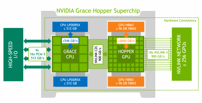
Long before NVIDIA acquired network hardware manufacturer Mellanox, the company had been developing its own local networking and interconnect technology using its short-distance NVLink standard. NVLink was initially introduced around 2016 in its Pascal architecture as a faster alternative to PCI-Express for achieving cache-coherent interconnects between GPUs. During this time, NVIDIA significantly increased NVLink’s bandwidth while expanding its coverage through NVLink switches and enhancing the ability to make electrical connections with adjacent nodes in the rack using NVLink. Today, NVIDIA views NVLink as one of its most important technologies, as it helps them address the challenge of scaling GPU systems to an entire rack, making their NVL72 rack with 72 GPUs possible.
Now, NVIDIA is working to push its NVLink technology further into the future by opening it up to semi-custom designs to meet customer flexibility needs. Currently, NVLink’s use cases are purely NVIDIA systems—primarily Grace Hopper and Grace Blackwell CPU+GPU configurations—and NVIDIA will open the NVLink ecosystem to semi-custom designs, allowing system vendors to replace NVIDIA CPUs or NVIDIA GPUs with custom hardware. This technology is aptly named NVLink Fusion, aimed at describing how it will allow third-party chips to integrate into the NVLink network.
Upon deeper investigation, it becomes clear that NVLink Fusion essentially bundles two different technologies. The first and most important is the semi-custom CPU—allowing non-NVIDIA CPUs to connect to NVIDIA GPUs via NVLink’s short-distance chip-to-chip variant NVLink C2C. Strictly speaking, this part of NVIDIA’s announcement is not new—the company opened NVLink C2C for custom silicon integration back at the 2022 GTC conference, so this is the next step in that plan. So far, we have not seen any (publicly announced) third-party chips released under the existing plan that support NVLink C2C, but that said, the development cycle for such hardware will take years, meaning the first CPUs supporting NVLink Fusion may launch under the old plan.
Regardless, NVIDIA is once again promoting the use of NVLink C2C in conjunction with third-party CPUs under the NVLink Fusion brand. Overall, this technology is relatively straightforward; hardware vendors simply need to obtain a license for NVLink C2C technology and integrate it into their own chips to connect to NVIDIA GPUs. These semi-custom chips will effectively replace the Grace CPUs in the current GB200/GB300 designs, with the semi-custom CPUs taking over Grace’s role. Previously, the only way to connect NVIDIA data center-grade GPUs was to use the PCIe versions of these cards (which seem to have completely disappeared), so this is effectively the next iteration of such hybrid vendor systems.
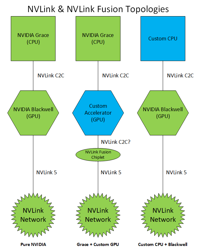
A more interesting and novel aspect of the NVLink Fusion announcement—and the part that requires new NVIDIA hardware—is pairing NVIDIA CPUs with third-party GPUs and accelerators using NVLink Fusion. Currently, this is not feasible on multiple levels: aside from NVIDIA’s own Hopper and Blackwell GPUs, there are no other accelerators that support NVLink C2C that can connect to Grace, and these GPUs are also where the full-featured NVLink 5 PHY resides, which allows Grace Hopper and Grace Blackwell nodes to connect to the NVLink network. In short, it is currently impossible to even insert third-party accelerators into the NVLink network, let alone insert Grace CPUs into all these networks.
To address this, NVIDIA is venturing into the Chiplet space. The company has developed an NVLink 5 Chiplet designed to be integrated into semi-custom accelerator designs, enabling these accelerators to gain NVLink 5 capabilities through NVIDIA’s Chiplet. Notably, NVIDIA has not authorized third parties to use NVLink 5; NVIDIA’s high-bandwidth interconnect technology remains proprietary. However, in the spirit of mixing Chiplets to build more powerful processors, NVIDIA provides chip manufacturers with a way to add NVLink 5 by adding NVIDIA’s Chiplet.
Currently, NVIDIA has not disclosed any hardware specifications for the chiplet itself. Therefore, it is unclear what its size and power consumption will be, or how many NVLink channels will be available in a chiplet, and whether a semi-custom accelerator can compete with a 200 GB GPU. NVIDIA has not clarified what technology will be used to connect the NVLink chiplet to the other parts of the accelerator—whether it will be NVLink C2C (the CPU link itself requires this technology) or another technology. However, if you are developing a high-performance accelerator and wish to connect it to the NVLink network, NVIDIA is finally making this possible.
Setting aside standards and topologies, NVIDIA has made it clear that NVLink Fusion will be viewed as an either-or technology. In other words, you can use it to integrate either a semi-custom CPU or a semi-custom GPU, but not both simultaneously. Therefore, system vendors will not be able to build NVLink-supported systems using both third-party CPUs and third-party GPUs—they will still need to install an NVIDIA chip on their nodes.
Currently, this seems to be entirely a licensing restriction rather than a technical limitation. Since all the real heavy lifting of NVLink 5 is done by the GPU—whether it is an NVIDIA GPU or an accelerator with an NVLink Fusion chiplet—the CPU does not play a critical role in the implementation of NVLink 5 (in fact, the CPU does not even use it). But since NVIDIA’s business is selling chips, they have no incentive to exclude themselves from future systems. Even providing chip designers with a way to replace NVIDIA GPUs with third-party accelerators seems relatively crazy, as most of NVIDIA’s profits currently come from GPUs.
Nevertheless, it is evident from the subtext that NVIDIA’s partners seem to be striving for some flexibility in rack designs. Grace Blackwell is not a panacea, especially with the future of AI accelerators still uncertain. But for whatever reason, the end result is the same: NVIDIA is finally opening up NVLink to external companies—at least a little.
Currently, the direct beneficiaries of this agreement will be Alchip, AsteraLabs, Marvell, and MediaTek, all of which have confirmed they are developing their own accelerators or participating in building accelerators integrated with NVLink Fusion. Meanwhile, Fujitsu and Qualcomm have both confirmed they are developing new CPUs that support NVLink Fusion, which can pair with NVIDIA’s GPUs. This includes Fujitsu’s next-generation high-end Armv9 processor Monaka and Qualcomm’s upcoming unnamed data center CPU. In both cases, CPU vendors hope to further enhance efficiency, and NVLink Fusion provides them with a pathway to access NVIDIA GPUs and their high-performance NVLink network architecture.
At the same time, Cadence and Synopsys are also participating as technical partners in the NVLink Fusion program, providing their IP blocks and design services to companies looking to build their own NVLink Fusion-supported hardware.
Reference link
https://www.servethehome.com/nvidia-announces-nvlink-fusion-bringing-nvlink-to-third-party-cpus-and-accelerators/
*Disclaimer: This article is original by the author. The content reflects the author’s personal views, and Semiconductor Industry Observation reprints it only to convey a different perspective, which does not represent Semiconductor Industry Observation’s endorsement or support of this view. If there are any objections, please contact Semiconductor Industry Observation.
END
Feel free to leave comments and engage in discussions!


Industry Community