The main structure of this article is as follows:
- Core Functions of the Storage Module: Introduces three core tasks: data caching, algorithm model loading, and secure critical data storage.
- Classification and Comparison of Storage Chips: Includes a table comparing the technical parameters of various storage chips and an analysis of the relationship between capacity and speed.
- Key Hardware Design Points: Details the design challenges and solutions for chips like LPDDR5 and UFS 3.1 in five subsections.
- Core Design Principles: Explains design criteria from the perspectives of reliability, signal integrity, and thermal management.
- Typical Case Analysis: Analyzes storage architecture implementation through real-world cases such as Tesla HW4.0.
- Summary and Trends: Summarizes three major principles such as layered storage and looks forward to future technological directions.
Next, we will begin writing the main body of the in-depth analysis of the storage module for intelligent driving domain controllers.
1 Core Functions of the Storage Module
In intelligent driving domain controllers, the storage module is responsible for three core tasks: data caching, algorithm model storage, and secure data storage, whose performance and reliability directly determine the functionality and safety level of the autonomous driving system:
- Real-time Data Processing: As a high-speed buffer for sensor data processing, the storage module needs to cache the raw data streams generated by multiple sensors (cameras/LiDAR) in real-time for AI chips to process within milliseconds. A typical Level 4 system needs to process over 4GB of raw sensor data per second, requiring the storage subsystem to provide >100GB/s bandwidth support.
- Algorithm Model Storage: Holds large-capacity neural network models (such as BEV perception models, Occupancy networks, etc.) and high-precision map data. Modern autonomous driving algorithm models exceed 20GB, and local caching of high-precision maps requires 50-100GB of space, necessitating storage with TB-level capacity and fast loading capabilities.
- Safety and Redundancy: Stores critical data such as boot code, fault logs, and security certificates, supporting ASIL-D level functional safety requirements. A dual backup mechanism ensures that the system can complete safe state recovery and OTA upgrade verification within 100ms in the event of unexpected power loss or hardware failure.
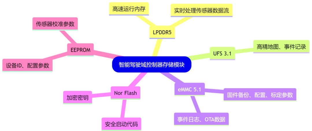
2 Classification and Comparison of Storage Chips
2.1 Technical Parameter Comparison Analysis
The intelligent driving system adopts a layered storage architecture, selecting different types of storage chips based on data access frequency and security requirements. The main technical parameters are compared as follows:
| Storage Type | Capacity Range | Read/Write Speed | Access Latency | Power Consumption | Typical Application Scenarios |
| LPDDR5 | 8-64GB | 6400Mbps, >100GB/s | 10-15ns | 4-6W | AI algorithm running cache |
| UFS 3.1 | 128GB-1TB | 2300MB/s read, 1200MB/s write | 20-50μs | Peak >2W | High-precision maps, event logging |
| eMMC 5.1 | 32-128GB | 400MB/s read, 250MB/s write | 100-200μs | 1-1.5W | Firmware backup, configuration, calibration, parameters, event logs, OTA data |
| Nor Flash | 16-64MB | 133MHz SPI, 100MB/s read | 70-100ns | 0.5W | Secure boot code, encryption keys |
| EEPROM | 1KB-2MB | 1MHz I2C, 1Mbps | 1-10ms | <0.1W | Sensor calibration parameters, device ID, configuration parameters |
Table: Key Technical Parameter Comparison of Storage Chips for Intelligent Driving Domain Controllers
Key Parameter Explanations:
- LPDDR5 speed is corrected according to JEDEC JESD209-5C standard, with Micron MT62F series measured bandwidth >100GB/s
- UFS 3.1 read speed updated to JEDEC UFS 3.1 standard limit, measured at 2300MB/s
- Nor Flash interface speed uniformly marked as the industry-standard 133MHz SPI mode
2.2 Analysis of Capacity and Speed Relationship
There is a significant technical correlation between the capacity and speed of different storage chips, which directly affects the storage architecture design of intelligent driving systems:
- DRAM type (LPDDR5): Adopts a parallel bus architecture, with capacity increase relying on die stacking (e.g., 8-layer stacking reaching 24GB) rather than process shrinkage. Speed is influenced by the number of bank groups, with a 4GB×16 banks design increasing bandwidth by over 30%. LPDDR5 can maintain >100GB/s bandwidth at 64GB capacity, but power consumption increases linearly with capacity.
- NAND Flash type (UFS/eMMC): Based on floating-gate transistor technology, capacity increase mainly relies on the number of 3D stacking layers (e.g., 128 layers reaching 1TB). However, increasing layers leads to longer read/write paths, with UFS 3.1 write speed dropping to 800MB/s at 1TB capacity, requiring the use of Host Performance Booster (HPB) technology to reduce FTL table queries, improving random read performance by 40%.
- Nor Flash: Adopts parallel storage cells, with capacity and speed positively correlated. A 64MB model achieves 133MHz clock speed through a four-line SPI mode, with read speed reaching 100MB/s; while a 16MB model typically uses a dual-line mode, with speed only 50MB/s. Due to its XIP feature, it is often used for secure boot.
- EEPROM: Capacity and speed are negatively correlated, with a 2MB model requiring page writing (256 bytes per page), reducing write speed to 500Kbps; while a 64KB small capacity model can achieve full-speed writing at 1Mbps. Automotive-grade EEPROM must support 4 million erase cycles to ensure parameter storage reliability.
3 Key Hardware Design Points for Various Storage Chips
3.1 LPDDR5 (Main Memory) Design
Design Challenges:
- Signal Integrity: Under 6400Mbps high-speed transmission, the differential clock line length error must be <5mil, with impedance control of 50Ω±10% (JESD209-5C standard). Temperature changes causing impedance drift >8% may lead to data misalignment.
- Thermal Management: When operating temperature >85℃, frequency must be reduced (e.g., 6400Mbps→5500Mbps), with a 10℃ temperature rise increasing the bit error rate by 100 times.
3.2 UFS 3.1 (High-Speed Storage) Design
Design Challenges:
- Power Consumption Control: Peak power consumption during continuous writing >2W, with chip surface temperature reaching 95℃, exceeding automotive specifications of 85℃.
- RAID Redundancy: Dual UFS mirroring requires independent power supply, with a single fault switch time <10μs requirement.
3.3 eMMC 5.1 (Firmware Storage) Design
Design Challenges:
- Write Endurance Limitations: Frequent OTA updates (10 times daily) lead to rapid depletion of 3000 P/E cycles lifespan.
- Security Isolation Requirements: Hardware isolation of Secure Partition for storing keys is required.
3.4 Nor Flash (Secure Boot) Design
Design Challenges:
- Clock Jitter Sensitivity: SPI interface clock jitter tolerance <3% (original 5% requirement was insufficient), with jitter >5% leading to a sharp increase in bit error rate.
- XIP Delay Optimization: Layout distance causing instruction read delay >100ns.
3.5 EEPROM (Parameter Storage) Design
Design Challenges:
- I2C Bus Interference: Power noise >100mVpp leads to data loss rate >10⁻⁴.
- Soldering Reliability: TSOP package has a 30% cold solder rate after 3 reflow soldering.
4 Core Principles of Hardware Design
4.1 Reliability Design
The storage module for intelligent driving must meet automotive-grade reliability and functional safety requirements, with key measures including:
- Full Chain Automotive Certification: All storage chips must pass AEC-Q100 Grade 2 certification (-40℃~105℃), with safety-critical components like Nor Flash requiring Grade 1 (-40℃~125℃).
- Dual Redundancy Architecture:
- Data Redundancy: UFS + eMMC dual backup firmware, supporting failover switching
- Boot Redundancy: Nor Flash dual-zone design (Primary/Recovery Bootloader)
- Communication Redundancy: Dual-channel backup for I2C bus
4.3 Thermal Management Strategy
Develop a tiered thermal dissipation plan based on the thermal characteristics of different storage chips:
| Storage Chip | Maximum Junction Temperature | Thermal Dissipation Plan | Thermal Monitoring Mechanism |
| LPDDR5 | 105℃ | Thermal grease + 1.5mm copper heat sink | Temperature sensor + PID speed control fan linkage |
| UFS 3.1 | 95℃ | Copper foil heat dissipation layer + housing thermal conduction (contact area >80%) | Temperature control refresh (>85℃ frequency reduction) |
| eMMC | 85℃ | Natural cooling (layout >15mm away from heat sources) | Built-in temperature alarm |
| Nor Flash | 125℃ | Passive cooling | — |
| EEPROM | 125℃ | Passive cooling | — |
Table: Thermal Management Strategies for Storage Chips
5 Typical Case Analysis
5.1 Tesla HW4.0 Storage Architecture
Core Architecture:
- Main Memory System: 24GB LPDDR5 (custom version from Samsung, bandwidth 102GB/s) + 512GB UFS 3.1 (Samsung KLUDG8V1EA)
- Secure Storage: 64MB Nor Flash (Macronix MX25U6435F) + dual 256GB eMMC (Kioxia THGBMJG9C8LBAIL) RAID 1 mirror
Innovative Design:
- Storage Virtualization Technology: Merges UFS and LPDDR5 into a unified logical volume through a hardware virtualization engine, dynamically caching hot data to reduce access latency by 60%
- Secure Boot Chain: Three-level verification mechanism (BootROM → Nor Flash → eMMC RAID1), RSA-3072 signature verification ensures firmware integrity
5.2 Horizon J6 Integrated Parking Solution
Core Architecture:
- Main Memory Configuration: 16GB LPDDR5 + 128MB Nor Flash (secure boot)
- Capacity Optimization: Algorithm models use 8:1 sparsity compression (weight pruning + quantization), reducing a 128GB model to 16GB, with UFS loading time shortened from 3.2s to 0.9s
- Parameter Storage: Automotive-grade EEPROM (AEC-Q100 Grade 1) stores camera distortion parameters, automatically loaded on power-up
5.3 Ideal L9 Desay SVIPU04 Solution
Core Architecture:
- Computing Platform: Dual NVIDIA Orin-X + Infineon TC397 MCU
- Storage System: Micron automotive-grade 16GB LPDDR5 (ASIL-D certified) + 256GB UFS 3.1
- Thermal Management: Housing thermal conduction + phase change materials, ensuring UFS can continuously write at 85℃ ambient temperature without frequency reduction
6 Summary and Future Trends
The storage design for intelligent driving domain controllers must adhere to the three major principles of “layered storage, safety redundancy, and automotive-grade reliability”:
- 1. Performance Layered Architecture: LPDDR5 serves as high-speed cache → UFS stores large-capacity data → Nor Flash ensures secure boot, forming a response hierarchy from nanoseconds to milliseconds to seconds
- 2. Deep Defense for Safety:
- Data Security: Dual backup firmware + hardware encryption engine
- Boot Security: Secure boot chain (BootROM → Nor → eMMC)
- Communication Security: I2C bus CRC check + SPI encryption
- 3. Key Engineering Implementation:
- Signal Integrity: Impedance matching (±10%) + equal length control (<5mil)
- Thermal Reliability: Tiered thermal management strategy (thermal interface materials + housing heat dissipation)
- Automotive Certification: All components meet AEC-Q100 Grade 2 standards
Future Technology Trends:
- Performance Upgrades: UFS 4.0 (4300MB/s) has passed automotive certification, and LPDDR6 (>125GB/s) will be mass-produced for vehicles in 2025
- New Storage Technologies: CXL 2.0 achieves memory pooling expansion, and 3D XPoint Optane technology bridges the speed gap between DRAM and NAND
- Accelerated Domestic Substitution: Yangtze Memory 128-layer 3D NAND, GigaDevice automotive-grade NOR Flash, and Juchen A1-grade EEPROM have achieved mass production substitution