In the Arduino ecosystem, the PCB design of shields is a professional task that requires comprehensive consideration of multiple factors. This article will detail the key points in the design of Arduino shields from a technical perspective of PCB layout design.1. Physical Dimensions and Mechanical ConstraintsStandard Size SpecificationsThe Arduino shield must strictly adhere to the form factor of standard Arduino boards. The standard size for the UNO shield is 68.6mm × 53.4mm, and when reserving stacking space, a minimum distance of 3mm between boards must be considered. During PCB design, care should be taken to avoid screw mounting holes and ensure that edge slots align perfectly with the main board.Stacking Design ConsiderationsFor multilayer board designs, a 4-layer stack structure is recommended:Top Layer: Signal layer and part of the power supplyInner Layer 1: Ground planeInner Layer 2: Power planeBottom Layer: Signal layer and part of the power supply2. Key Signal Routing StrategiesHigh-Speed Signal ProcessingI2C, SPI, and other bus signals should adopt a length-matched design.Differential signals must strictly control impedance matching (90~100Ω).Clock signal routing should avoid sharp angles, using 45-degree turns.Power Integrity DesignDecoupling capacitors should be placed between VCC and GND, using 0402/0603 packages.High current paths should use multiple vias in parallel to reduce equivalent resistance.Local power decoupling networks should be set up around key components.3. Component Layout PrinciplesInterface Position PlanningStrictly follow the standard pin definitions of Arduino.Ensure that the expansion interface accurately corresponds to the Arduino main board pins.Leave sufficient space for manual soldering.Thermal Design Considerations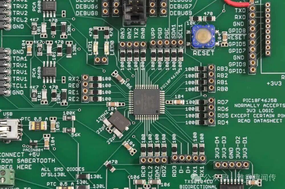 Leave enough copper area for heat dissipation around power devices.Heat-sensitive components should be kept away from heat sources.Design heat dissipation hole arrays if necessary.4. EMC Design PointsElectromagnetic Compatibility OptimizationKey signals should adopt a ground plane surrounding design.High-frequency circuit areas should have grounding fences.Analog and digital circuits should be laid out in separate zones to reduce interference.Interference Resistance DesignKey signal lines should avoid running parallel to power lines.Use a star grounding topology.Set up a protective grounding ring at the board edge.5. Manufacturing Process AdaptabilityDFM Design SpecificationsThe minimum line width/spacing should not be less than 6 mil.Via diameter is recommended to be above 0.3mm.Component layout should reserve space for automatic placement.Testing and Maintenance ConvenienceReserve test points.Design test pads for key networks.Silkscreen layer should indicate component polarity and key parameters.Conclusion:The PCB design of Arduino shields is a system engineering task that requires balancing multiple requirements. Designers need to ensure basic functionality while fully considering signal integrity, power integrity, EMC characteristics, and manufacturing convenience across various dimensions. A good PCB layout is a crucial guarantee of product reliability, and it is recommended that designers invest sufficient time in layout planning and simulation verification in the early stages.Would you like me to explain any specific technical terms or concepts mentioned in this article?12:41