How can traditional printing processes break through physical limits under the stringent requirement of a solder paste thickness deviation of only ±15μm? The modern SPI (Solder Paste Inspection) closed-loop system reduces the defect rate from traditional manual sampling of 3500ppm to below 50ppm through 3D laser scanning and real-time feedback control, becoming the first line of quality defense in SMT production lines.

Physical Limits and Breakthrough Paths of Solder Paste Printing
The five core variables of the printing process
- Blade Pressure The optimal pressure range for stainless steel blades is 50-100N/cm, with pressure fluctuations >5% leading to a 12% decrease in filling rate.
- Printing Speed Within the range of 30-80mm/s, the rheological properties of solder paste exhibit shear-thinning effects (viscosity decreases by 40%).
- Separation Speed A stencil release speed of 0.1-0.5mm/s can reduce the occurrence of tailing defects, which is exponentially related to solder paste viscosity (formula:
<span>V_sep=K×η^(-0.7)</span>). - Environmental Temperature and Humidity The best rheological stability of solder paste occurs at a temperature of 23±2℃ and humidity of 45±10%RH (IPC-7525 standard).
- Stencil Life After 50,000 prints, laser-cut stencils experience wear in opening dimensions, leading to a solder paste volume deviation of up to 8%.
Non-Newtonian Fluid Control Technology Solder paste, as a Bingham fluid, has a dynamic relationship between yield stress τ and viscosity η given by:
τ = τ_y + η(du/dy) - Thixotropic Recovery Solder paste needs to rest for 120-180 seconds after printing to rebuild its thixotropic structure (recovery rate of 85%).
- Nanoparticle Additives Adding 0.1wt% silica nanoparticles can enhance anti-collapse properties (standing height increases by 30%).

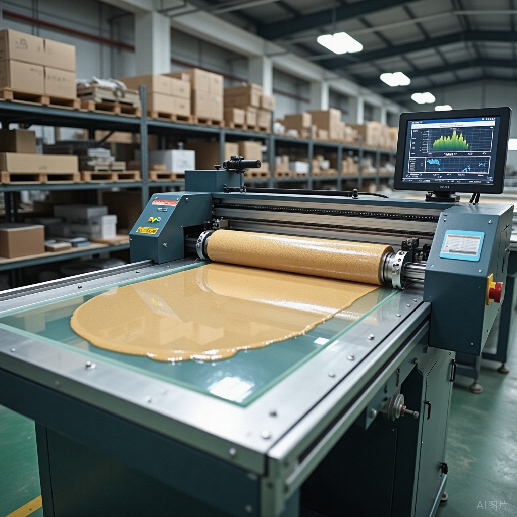
SPI Closed Loop System Architecture
Why can’t 2D inspection identify “virtual thickness” defects? Traditional optical inspection only measures planar dimensions, while 3D laser confocal technology can detect height direction with a resolution of 0.5μm (meeting ISO-9001 Class B standards).
Comparison of Core Sensor Technologies
| Technology Type | Principle | Accuracy (Z-axis) | Speed (points/second) |
|---|---|---|---|
| Laser Triangulation | Laser Displacement Sensor | ±5μm | 50,000 |
| White Light Interferometer | Phase Shift Interference | ±0.1μm | 10,000 |
| Structured Light | Grating Projection Phase Decoding | ±2μm | 100,000 |
Real-time Feedback Control Logic
- Data Acquisition Each PCB scans 3,000-5,000 feature points (taking <5 seconds).
- Defect Classification
- Insufficient Volume (<80% of target value)
- Bridging (spacing between adjacent pads <50μm)
- Offset (position error >25μm)
- Blade Pressure PID adjustment (response time <0.1 seconds)
- Adaptive compensation for printing speed (gradient descent algorithm)

Solutions for High-Difficulty Application Scenarios
Ultra-fine Pitch QFN Packaging
- Step Stencil Design 0.08mm thick area for peripheral fine leads (0.3mm pitch), 0.12mm thick area for central heat sink pads.
- Nanocoated Stencils Diamond-like carbon (DLC) coating reduces release resistance (friction coefficient <0.1).
Flexible Circuit Board Printing
- Vacuum Adsorption Platform Local vacuum of -85kPa prevents substrate deformation (warpage control <0.1mm/m²).
- Dynamic Compensation Algorithm Real-time Z-axis leveling based on strain gauge data (accuracy ±3μm).
Defect Root Cause and Process Capability Analysis
Why does the solder paste volume fluctuation of 0402 components exceed that of 0603 by 40% under the same parameters? The area-perimeter ratio change of small pads enhances the rheological boundary effect (Reynolds number Re <0.01).
Critical Process Indicators (CPK)
| Parameter | Target Value | 6σ Control Limits | CPK≥1.33 Requirement |
|---|---|---|---|
| Solder Paste Thickness | 100±15μm | 70-130μm | Measurement Points >30 |
| Volume Coverage Rate | 95-105% | 85-115% | Zone Statistics |
| Position Offset | <25μm | <50μm | Point-by-Point Comparison |
Defect Tracing Methods
- Fishbone Diagram Analysis Materials (solder paste batch differences), machines (blade wear), methods (release speed settings), environment (temperature and humidity drift).
- Pareto Chart Data shows that 70% of bridging defects are caused by improper stencil cleaning.
Technical and Economic Validation
Is investing in the SPI closed-loop system worthwhile? Data from an automotive electronics factory indicates:
- Throughput Rate Improvement Increased from 92% to 99.5% (annual savings of $280,000 in rework costs).
- Material Waste Reduction Solder paste usage decreased by 18% (annual savings of $75,000).
- OEE Improvement Overall equipment efficiency increased by 11% (equivalent to an additional production capacity of 1,200 hours/year).
Cutting-edge Development Directions
- AI Predictive Maintenance Predicting blade lifespan through vibration frequency spectrum (accuracy >90%).
- Digital Twin Simulation Simulating solder paste flow field based on ANSYS Fluent (measurement error <5%).
- Quantum Dot Marking Incorporating fluorescent nanoparticles into solder paste for full-process traceability.
Interactive Topics:
- When printing Micro LED arrays with a 0.2mm pitch, how to balance stencil opening rate and structural strength?
- What are the essential differences in thixotropic properties between lead-free solder paste (SAC305) and leaded solder paste (Sn63Pb37)?
- For thick copper PCBs (≥3oz), what stencil design can avoid insufficient filling caused by the “copper wall effect”?
- In space electronics manufacturing, how to address the sudden changes in solder paste rheological properties in microgravity environments?
- How can SPI data be deeply integrated with MES systems for real-time Cpk monitoring?
Topic Tags:#SolderPasteRheology #SPIClosedLoop #NanocoatedStencils #ProcessCapabilityIndex #DigitalTwin

 Chew on this, we hope our content inspires you, and you can also follow our other recommended channels.Capture every little happiness in life, starting today, let the unknown beauty be within reach. Choose your favorite items and embark on a wonderful journey.!
 Follow and like for continuous good luck! Clickto see your best look!