In the production of circuit boards, the quality of wave soldering is extremely important. How to improve the quality of wave soldering is a key issue that every wave soldering equipment engineer, electronic manufacturing process engineer, and electronic manufacturing manager needs to consider.
Improving the quality of wave soldering is a systematic project that requires comprehensive optimization from multiple aspects, including equipment, processes, materials, PCB design, and operational maintenance.
1. Equipment and Process Parameter Optimization (Core)
1. Flux Management
Coating Amount: Ensure that the flux is applied evenly and in the right amount. Too little can lead to poor soldering (bridging, cold solder), while too much can produce excessive residues, potentially causing corrosion or electro-migration. Using a quantitative spraying system is more precise than foaming or brushing.
Activity and Type: Choose the appropriate type of flux (e.g., RMA, RA, no-clean) based on the cleanliness of the PCB, component reliability requirements, and product specifications. Regularly test the specific gravity and acid value of the flux to prevent failure.
2. Preheat Temperature
Function: Evaporate the solvent in the flux to prevent solder splashing; activate the flux activity and remove oxides; reduce thermal shock when the PCB contacts the solder wave.
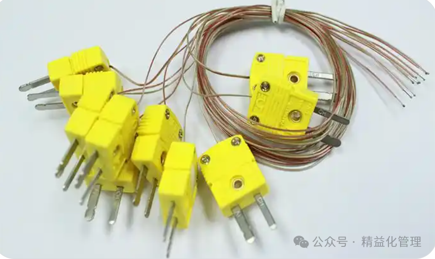
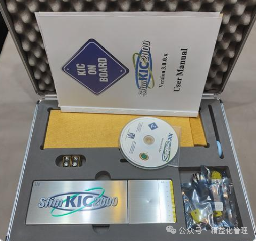
Control: Typically, the surface temperature of the PCB after preheating should reach 90-120°C (adjust according to flux specifications). Insufficient preheating can lead to solder balls and bridging; excessive preheating can deactivate the flux too early, resulting in poor wetting. Use a furnace temperature tester (like KIC) to regularly measure and optimize the preheating curve.
3. Solder Pot Temperature
Lead-free Process: Typically set between 255°C – 265°C. If the temperature is too low, the flowability is poor, leading to icicles and bridging; if too high, it accelerates dross production, damages components and PCBs, and may reduce solder joint reliability.
Monitoring: A precise thermometer must be used to regularly calibrate the actual furnace temperature to ensure it matches the set value.
4. Wave Shape and Parameters
Wave Height: Typically controlled at 1/2 – 2/3 of the PCB thickness. Too high can lead to bridging, too low can lead to cold solder.
Immersion Time: Typically controlled at 3-5 seconds. Too short a time results in insufficient wetting; too long a time results in excessive heat, which may damage components and increase dross and copper dissolution.
Transfer Speed/Angle: Speed must be adjusted in coordination with preheat temperature and solder pot temperature. If the speed is too fast, preheating and soldering will be insufficient; if too slow, thermal input will be excessive. The transfer angle (typically 5°-7°) is crucial for detaching from solder points and reducing bridging. An appropriate angle helps the liquid solder flow back smoothly.
Wave Stability: Ensure that the wave pump operates smoothly, with no turbulence or jumping in the wave, otherwise it will lead to unsmooth solder joints and oxidation residues being entrained.
2. Material Control
1. PCB Quality
Solderability of Pads and Holes: Ensure that the PCB surface treatment (e.g., HASL, ENIG, OSP) is good, without oxidation or contamination. The storage environment should be moisture-proof and oxidation-proof.
Design: Comply with DFM (Design for Manufacturability) requirements, such as pad spacing, steal pad design, component layout, etc.
2. Components
Solderability: Component leads or solder ends must not have severe oxidation or contamination.
Temperature Resistance: All components must withstand the thermal process of wave soldering.
3. Solder Alloy
Purity: Use high-purity solder bars and regularly test the chemical composition of the solder pot (e.g., excessive copper or iron content can affect soldering quality, requiring regular skimming or replacement of solder).
Alloy Type: Choose the appropriate alloy based on product requirements (e.g., SAC305, SnCuNi, etc.).
3. PCB Design (DFM – Design for Manufacturability)
Many quality issues stem from poor design.
1. Component Layout: Avoid placing tall components next to small components, as this can create a “shadow effect” that obstructs solder flow, leading to cold solder on small components.
2. Pad and Solder Mask Design:
The solder mask should not have deviations and must be accurately aligned with the pads.
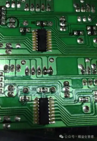
For densely pin-packed components (e.g., connectors), using steal pads is the most effective method to prevent bridging.
3. Through-Hole Design: The gap between component holes and pins should be appropriate (typically larger by 0.2-0.4mm) to facilitate solder wicking.
4. Thermal Relief: For large copper foil areas in through-hole components, use thermal isolation design to prevent rapid heat loss that can lead to cold solder.
4. Operation and Maintenance
1. Daily Maintenance
Regularly clean solder dross: Clean solder dross daily or per shift to prevent oxidation residues from being pumped into the wave, affecting solder joint quality and wave stability.
Clean the flux system: Prevent nozzle clogging and solidified residues.
Check chains and claws: Ensure the transport system operates smoothly, without shaking, and at the correct angle.
2. Process Monitoring
First Article Inspection (FAI): Strictly check the quality of the first article board at the start of each shift or when changing lines.
Statistical Process Control (SPC): Continuously monitor and record key parameters (e.g., preheat temperature, solder pot temperature) to promptly identify trends and anomalies.
Regularly use furnace temperature testers: Measure the actual temperature curve of the PCB passing through the furnace to ensure it meets the process window.
5. Common Defects and Targeted Solutions
Bridging:
Check/optimize the transfer angle.
Increase/optimize steal pad design.
Appropriately lower wave height.
Check if the flux is insufficiently active or applied.
Slightly increase solder pot temperature or decrease transfer speed.

Cold Solder/Skipping:
Check the solderability of components and PCB pads.
Appropriately increase solder pot temperature or decrease transfer speed.
Check if the wave height is too low.
Check if the flux application is normal.
Check for shadow effects and optimize layout.
Solder Balls:
Ensure sufficient preheating to completely evaporate the solvent in the flux.
Check if the flux application is excessive.
Check if the PCB or components are damp, and pre-bake if necessary.
Icicles:
Appropriately increase solder pot temperature or decrease transfer speed.
Check the activity of the flux.
Confirm if the transfer angle is appropriate.
The key to improving wave soldering quality lies in:
1. Stable and optimized process parameters (temperature, time, speed, angle).
2. Good equipment condition and strict maintenance.
3. PCB design that complies with DFM standards.
4. Qualified and consistent materials (PCBs, components, solder, flux).
5. Systematic process monitoring and continuous improvement.
It is recommended to establish a detailed control plan that defines, monitors, and records each critical point to systematically enhance and maintain the quality of wave soldering.