To effectively reduce power consumption, design engineers need to approach from multiple levels, including architecture design, circuit optimization, process selection, and more. This article will focus on circuit-level low-power design, introducing several common optimization methods, such as Clock Gating, Toggle Rate Optimization, Area Optimization, and Memory Low Power Management, to help engineers more efficiently reduce power consumption and improve chip energy efficiency in practical designs.
1. Clock Gating
1.1 Overview of Clock Gating
(1) Module-based clock gating: In specific scenarios, if a module does not need to operate, its clock can be turned off to reduce power consumption.
(2) Register-based clock gating: For modules that cannot be completely turned off, the number of register toggles can be reduced to lower power consumption.
1.2 Advantages of Clock Gating
The clock tree typically consists of a large number of buffers and inverters, and the clock signal is the signal with the highest toggle rate in the entire design, resulting in a significant portion of power consumption attributed to the clock tree. Using clock gating can reduce clock toggling behavior, thereby lowering dynamic power consumption.
1.3 Implementation of Clock Gating
(1) Module-based gating: Instantiate vendor-supplied ICG (Integrated Clock Gating) standard cells.
(2) Circuit-based gating: EDA tools can automatically insert gating logic, for example, when the number of bits in the register is greater than or equal to 4 or 8 (empirical value, adjustable). Generally speaking, the higher the process technology, the larger the number of bits.
always @(posedge clk or negedge rst_n)begin if(!rst_n) begin data_hold <= {WID{1'b0}}; end else if (vld == 1'b1) begin data_hold <= data; end else ;end2. Circuit Optimization to Reduce Toggles
2.1 Pre-optimization Scheme
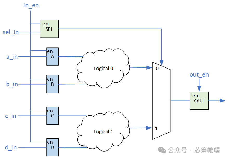
In the design shown above, even if the output is invalid, data may still toggle, causing additional power consumption. If out_en is invalid but in_en is still valid, unnecessary operations will still occur.
2.2 Optimization Scheme (Operand Isolation)
(1) Control data input and multiplexer output through sel_in.
(2) When out_en is invalid, also make in_en invalid to reduce toggles.
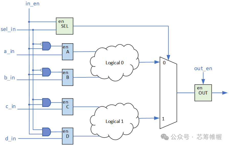
3. Area Optimization to Reduce Power Consumption
3.1 Original Scheme
The design includes 32 sets of register templates that perform logical operations with calc_data[31:0]. However, only one set of operation results is ultimately output, leading to redundant logical operations.
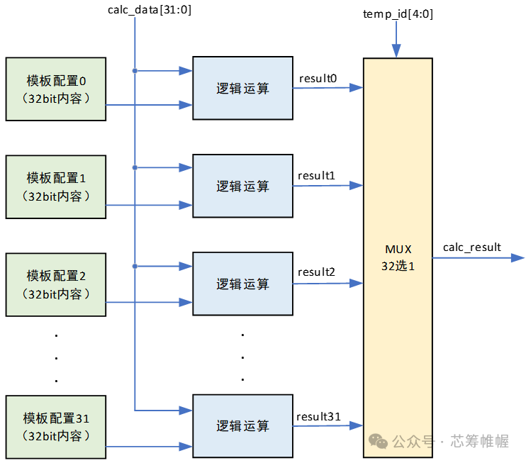
3.2 Optimization Scheme
(1) First use temp_id to select the required data, then perform logical operations.
(2) Reduce logical operations to one instance, thus lowering area and power consumption.
4. Non-resetting Registers and Hold Circuits
Using non-resetting registers can reduce power consumption, but careful analysis is needed to determine if initial values are required.
(1) Control logic typically needs to be reset, while data storage (such as data or memory read/write addresses) may not need resetting.
(2) For example, vld uses a resetting register, while data uses a non-resetting register, and when vld=1, it is stored.
always @(posedge clk or negedge rst_n)begin  if(!rst_n)    begin        vld_d1 <= 1'd0;        vld_d2 <= 1'd0;end  else    begin        vld_d1 <= vld   ;        vld_d2 <= vld_d1;  endend
always @(posedge clk)begin  if(vld)    begin        data_d1 <= data   ;        data_d2 <= data_d1;  end  else ;end
5. Dynamic CG for Register Forms
For software-accessible registers (such as configuration registers, status registers), when the software does not access them, the register clock can be turned off through clock gating to reduce power consumption. Use the read/write signals of the register as the enable signal for clock gating. When the software does not access the register, clock gating is performed.
6. Memory Low Power Management
Utilize the DS (Deep Sleep), LS (Light Sleep), and SD (Shut Down) features of memory:
(1) Large-capacity MEM uses BANK management, turning off some BANKs based on application scenarios to reduce power consumption.
(2) When SRAM is not accessed after startup, it can enter the SD state, saving power.
-
6.1 Memory Sleep Modes
-
(1) Light Sleep: Retains data, leakage reduced by 80%;
-
(2) Deep Sleep: Data lost, leakage reduced by 99%.
-
6.2 Example
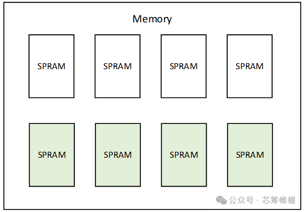
The module design requires a memory (8M). After considering address management and balanced processing, this memory is divided into 8 blocks for management. In a full bandwidth scenario, all 8 blocks of SRAM need to be operational. In a half bandwidth scenario, only 4 blocks of SRAM need to work, while the remaining 4 can enter low power mode. As shown in the figure below:
7. SPRAM Replacing TPRAM
(1) SPRAM has higher integration, usually with smaller area and lower power consumption:
In most cases, SPRAM with the same bit count will have a smaller area and lower power consumption than TPRAM. When the RAM depth is small, the area and power consumption of SPRAM and TPRAM with the same bit count may also be similar; specific situations should refer to the vendor’s RAM manual.
(2) Synchronous FIFO design optimization (to be detailed in a future article):
-
Use two single-port RAMs instead of dual-port RAM, with odd/even ping-pong access;
-
Simultaneous read and write of odd and even will not conflict and can be directly operated;
-
Simultaneous read and write of odd and even at the same time must stagger reads and writes to avoid conflicts.
8. Resource Sharing
Reduce duplicate logic and improve resource utilization. For example, assign complex logic used multiple times to a variable to reduce repeated calculations.
// Before optimization: 32 instances of the same comparison logicif (pcntr == (cnt<<1 + cnt)) ... // After optimization: global signal reusewire pcntr_eq;assign pcntr_eq = (pcntr == cnt*3);Tools may automatically optimize; if complex logic statements appear multiple times, this method can be used to declare them in advance. Although it may not reduce resources or lower power consumption, it improves code readability.
9. State Encoding
For frequently changing signals, encoding can be used to reduce switching activity.
For example: use Gray code instead of binary code to reduce toggles, thereby lowering power consumption.
10. Selection of Parallel and Pipelining
10.1 Parallel Processing
(1) Reduces system operating frequency, which may lower power consumption.
(2) A trade-off between area and power consumption must be considered.
10.2 Pipelining Technology
(1) Tasks are executed in stages, reducing instantaneous power peaks.
(2) Power consumption is more evenly distributed, reducing power spikes.
11. Low Power Design Verification
Must establish the following checks:
(1) Clock gating coverage > 95%;
(2) Non-resetting register simulation initialization verification;
(3) Timing margin for power mode switching;
(4) Assertions on memory low power mode interfaces.
Low power design is an essential aspect in chip design that cannot be ignored. Optimizing from various levels such as clock management, data toggle optimization, memory management, and logic sharing can effectively reduce dynamic and static power consumption. In practical projects, reasonably applying techniques such as clock gating, operand isolation, state encoding, and pipelining optimization, along with the automatic optimization capabilities of EDA tools, will significantly enhance the energy efficiency ratio of chips.
I hope this article provides valuable insights and references for engineers, aiding in more efficient low power design. Feel free to share your thoughts and experiences in the comments!