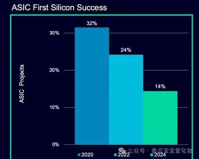
Have you ever touched a freshly baked smartphone chip? That silicon wafer the size of a fingernail is now a hot potato. According to Siemens EDA’s latest data, the global chip yield rate has halved for the first time—plummeting from 24% two years ago to just 14% now, more shocking than your child’s declining monthly exam scores. This is not just an ordinary technical bottleneck; the entire semiconductor industry is facing an unprecedented upheaval in twenty years.
When TSMC engineer Xiao Wang stares through the microscope at the wafer factory at three in the morning, what he is handling is no longer a traditional “complete chip”. Now, a palm-sized package must cram in a CPU, GPU, AI accelerator, RF module, and several other chiplets, each potentially from different process nodes. It’s like having a dozen actors speaking different dialects performing on the same stage; a slight misstep could turn it into a disaster scene. Synopsys CEO Aki said it best: “Designing chips now is like conducting a symphony orchestra, but every musician is improvising.”
The verification phase has become a time-consuming black hole. Three years ago, verifying a 5nm chip could be done step by step, but now, facing the complex structure of 3D stacking, engineers must simultaneously handle over a dozen parameters such as thermal conduction, electromagnetic interference, and signal delay. Matt Graham from Cadence Electronics likened it to: “Previously, verification was like an annual inspection for a car; now it’s a comprehensive check-up for a space shuttle.” Even more challenging is the rapid iteration speed of AI chip software; just as the hardware design is finalized, the algorithm team updates three versions, forcing the verification team to perform the daily act of “changing wheels while chasing a train.”
Veterans in the industry are starting to reminisce about the “golden age”. Twenty years ago, when making 130nm chips, engineers could sip coffee while watching waveform diagrams. Now, with 3nm processes, the design rule documents exceed 8,000 pages, three times thicker than “Dream of the Red Chamber”. Although EDA tools have incorporated AI assistance, seasoned engineers have found that AI-generated test cases often miss critical boundary conditions—much like using ChatGPT to draft a legal contract that looks good but is fraught with hidden pitfalls.
The pit of safety verification is even deeper. Automotive chips must withstand extreme temperatures from -40°C to 125°C, while also defending against hackers, radiation, and electromagnetic pulses. Axiomise’s Dalbari shared a personal experience: a certain car manufacturer’s autonomous driving chip performed well in simulation but failed during real-world testing due to reflections from roadside billboards. Such bizarre bugs leave the verification team exclaiming, “We can’t do this,” forcing them to apply for a second tape-out.
Industry veterans are brewing big moves. Synopsys’s “AI co-pilot” system can boost verification efficiency by 20 times, but senior engineer Lao Zhang complained: “This thing is like Level 2 autonomous driving; it’s fine for assistance, but if you let it take over completely, it might turn the design into abstract art.” Even more aggressive is the quantum verification algorithm that Google is testing, which theoretically can compress three months of work into three hours, but first, you need to understand how to use quantum entanglement.
Packaging technology is also evolving rapidly. Intel’s Foveros 3D stacking can layer 12 chips into a sandwich, while TSMC’s CoWoS solution allows chips of different processes to party on a silicon interposer. However, these flashy operations bring new problems—when your chip thickness exceeds 1mm, heat dissipation becomes a barbecue grill, necessitating the use of liquid metal cooling and microchannel technologies. An engineer wryly remarked: “Now making chips requires knowledge of materials science, fluid dynamics, and a bit of mysticism.”
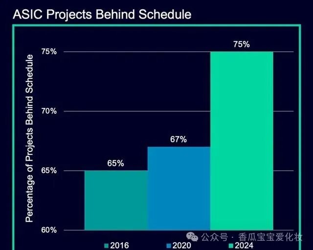
This chip crisis hides deeper industry logic. Ten years ago, making chips was a “ten-year sword sharpening” process; now it has turned into “three generations in a month”. Consumer electronics giants are pushing suppliers to iterate at breakneck speed, resulting in a surge in tape-out numbers. Industry insiders reveal that 60% of the actual R&D costs for a flagship chip from a major smartphone manufacturer are burned on repeated tape-outs. This is not R&D it’s clearly throwing money at probability.
Amidst the undercurrents, a new industrial landscape is taking shape. TSMC has begun charging a “complexity surcharge”, directly discouraging small clients; Intel has bundled advanced packaging capacity with Amazon Cloud, launching “tape-out as a service”; and China has seen the emergence of several Chiplet alliances, attempting to use modular design to overtake competitors. The most surreal scene in this chaotic battle is a startup using a 14nm chip to achieve 7nm performance, cutting costs by 40%, infuriating traditional giants.
Standing under the dome of the wafer factory, watching robotic arms precisely grasp silicon wafers, you suddenly realize: humanity is approaching the singularity of semiconductor technology. When chip complexity exceeds the human brain’s understanding, and AI design tools begin to iterate autonomously, the era when the first tape-out success rate reached 30% may become a legend. However, from another perspective, this crisis is catalyzing a new technological revolution—just as the moon landing race birthed integrated circuits, today’s tape-out dilemma may be nurturing disruptive innovations that change the game.