Introduction
In the modern electronics industry, IC substrates and PCBs shine like twin stars; they serve as the “skeleton” of electronic devices and the “nervous system” for signal transmission. IC substrates, as the core material for integrated circuit packaging, play a crucial role in bridging the chip and the PCB motherboard. Meanwhile, PCBs are known as the “mother of electronic products,” an indispensable foundational carrier for all electronic devices. With the explosion of AI technology, the proliferation of 5G communications, and the rise of new energy vehicles, these two technological fields are facing unprecedented development opportunities and challenges.
Currently, the global electronics industry is at a critical juncture of technological transformation. On one hand, the demand for ultra-high-density interconnections in AI chips is pushing IC substrate technology towards extreme precision, with line widths/spacing breaking through from the traditional 50μm to 5-6μm, and challenging the 3μm technical limit by 2025. On the other hand, applications such as 5G base stations, servers, and new energy vehicles are driving a surge in demand for high-frequency, high-speed PCBs, pushing the industry towards high-end and intelligent development. Meanwhile, geopolitical factors have exacerbated supply chain risks for key materials, with Japanese companies monopolizing core materials such as ABF films, making domestic substitution an urgent need for industry development.
This study aims to deeply analyze the differences and connections between IC substrates and PCBs in terms of technical specifications, manufacturing processes, market landscape, and application scenarios, providing comprehensive decision-making references for electronic engineers, industry investors, and policymakers. Through systematic comparative analysis of the two technological fields, it reveals their different positions in the electronics industry value chain and the key trends in future technological evolution.
1. In-Depth Comparison of Technical Specifications and Design Characteristics
1.1 Differentiated Material Systems
IC substrates and PCBs exhibit significant technical stratification in their material systems. The material systems of IC substrates are mainly divided into three categories: rigid substrates, flexible film substrates, and co-fired ceramic substrates, with rigid substrates occupying the majority of the market space. Among rigid substrates, the main materials include BT resin, ABF resin, and MIS resin, each with its unique performance characteristics and application scenarios. BT resin substrates, developed by Japan’s Mitsubishi Gas Chemical Company, are important materials for high-density interconnects (HDI), build-up multilayer boards (BUM), and packaging substrates. BT resin is synthesized from bismaleimide (BMI) and cyanate ester (CE) resins, exhibiting excellent thermal stability, mechanical strength, and electrical performance, with a glass transition temperature (Tg) reaching 200-300°C and a long-term heat resistance temperature of 160-230°C. BT substrates are dimensionally stable, resistant to thermal expansion and contraction, and are primarily used in applications such as mobile phone MEMS, storage, RF, and LED chips. ABF substrates (Ajinomoto Build-up Film), developed by Japan’s Ajinomoto Company, are a build-up film material characterized by higher hardness, thinner thickness, and good insulation, suitable for fine lines, high layer counts, and multi-pin IC packaging. The core advantage of ABF material lies in its ultra-high wiring density, with line widths/spacing as low as 5-20μm, excellent inter-layer insulation, and compatibility with silicon chips (CTE about 3ppm/°C) to reduce thermal stress. In contrast, the material system of PCBs is relatively standardized. FR-4 (epoxy glass cloth laminate) is the most commonly used PCB substrate, made of glass fiber cloth and epoxy resin, featuring flame retardancy (FR=Flame Retardant), low cost, and high mechanical strength, suitable for most electronic devices. The Tg value of FR-4 is typically between 130-140°C, with high Tg versions exceeding 170°C, suitable for high-temperature environments. Additionally, PCBs also use high-performance materials such as BT resin, which has a Tg as high as 250-300°C and a thermal expansion coefficient (CTE) of only 2-5ppm/°C, significantly lower than FR-4’s 11-14ppm/°C.
1.2 Technical Gap in Line Width/Spacing Precision
There is an order of magnitude difference in line width/spacing precision between IC substrates and PCBs, which directly determines their different positioning in electronic systems. IC substrates require extremely high line width/spacing precision, with high-end products entering the 5-6μm range, and challenging the 3μm technical limit by 2025. The core process of ABF substrates uses ABF film as the inter-layer medium, achieving micron-level lines through the semi-additive process (mSAP), with line widths/spacing reaching 5μm and hole diameters ≤30μm, requiring extremely high precision for exposure and etching equipment. In contrast, the line width/spacing precision of PCBs is relatively relaxed. For standard FR-4 boards, the minimum line width/spacing supported by conventional processes is 6mil/6mil (approximately 0.15mm/0.15mm), while high-precision processes can achieve 3mil/3mil (0.076mm/0.076mm). The minimum line width/spacing for high-density interconnect (HDI) PCBs can reach 3mil (0.075mm). Traditional PCBs typically have line widths/spacing above 50μm, with 50μm/50μm considered high-end products.
This precision difference reflects the different functional positioning of the two in electronic systems. IC substrates are primarily used to connect individual IC chips, requiring high-density interconnections between chip pins and external circuits; whereas PCBs are used to connect multiple electronic components, forming a complete circuit system, with relatively relaxed line width/spacing requirements but higher complexity in overall wiring.
1.3 Technical Evolution of Layer Structure and Board Thickness Specifications
In terms of layer structure, both IC substrates and PCBs are trending towards higher layer counts and ultra-thin designs, but their technical paths exhibit significant differences. IC substrates have a wide range of layer counts, from 1 layer to over 90 layers, with board thickness typically ranging from 0.3-7mm. Currently, mainstream products are 14-20 layer structures, while the latest AI chips, such as NVIDIA’s Rubin Ultra solution, are expected to exceed 30 layers in their ABF substrates. The layer structure of PCBs is relatively standardized, with common multilayer boards typically being 4-layer or 6-layer, and complex multilayer boards reaching dozens of layers. Multilayer boards (≥4 layers) are formed by alternating stacking multiple signal layers, power layers, and ground layers, connected through blind holes/buried holes/vias, suitable for high-speed, high-density circuits, such as mobile phone motherboards and server backplanes. The most commonly used board types in communication devices are 8-16 layer high multilayer boards, while 6-layer and 8-16 layer high multilayer boards are most commonly used in service/storage devices.
1.4 Technical Comparison of Key Performance Indicators
IC substrates and PCBs exhibit significant differences in key performance indicators such as thermal expansion coefficient (CTE), dielectric constant, and thermal conductivity, which directly affect their application scenarios and technical requirements. In terms of thermal expansion coefficient, the material systems of IC substrates show diverse characteristics. Ceramic substrates have the lowest CTE, around 6-8ppm/°C, which matches best with the thermal expansion coefficient of silicon chips (about 3ppm/°C); rigid packaging substrates (BT/ABF) have a CTE of about 13-17ppm/°C; and flexible packaging substrates have a CTE range of 13-27ppm/°C. In contrast, the X/Y axis CTE of PCB’s FR-4 material is 14-17ppm/°C, but the Z-axis CTE can be as high as 40-60ppm/°C, exhibiting significant anisotropy. The CTE of BT material is only 2-5ppm/°C, far lower than that of FR-4, which gives BT material better dimensional stability in high-temperature environments. In terms of dielectric constant, IC substrates typically exhibit superior high-frequency performance. The dielectric constant (Dk) of ABF substrates is about 3.0-3.3, enabling more precise impedance control and lower signal delay. In contrast, the dielectric constant of FR-4 is 4.5-4.8, while high-frequency materials have a dielectric constant of 2.2-3.5, flexible materials range from 3.2-3.5, and metal-based materials range from 3.0-3.5. The dielectric constant of IC substrates is typically 3.5-4.2, outperforming PCB’s 4.0-4.7 in high-frequency performance. In terms of thermal conductivity, ceramic substrates perform the best, with thermal conductivity 10-100 times that of resin substrates, capable of withstanding temperatures above 500°C. The thermal conductivity of FR-4 substrates is about 0.3W/m·K, while ceramic substrates like aluminum nitride can reach 2.8W/m·K, which is 9 times that of FR-4. This high thermal conductivity characteristic makes ceramic substrates particularly suitable for high power density applications.
2. Differentiated Paths of Manufacturing Processes
2.1 Semiconductor-Level Manufacturing Process of IC Substrates
The manufacturing process of IC substrates represents the highest standard of PCB technology, epitomizing the deep integration of semiconductor packaging technology and PCB manufacturing technology. Its core processes include semi-additive process (SAP) and modified semi-additive process (mSAP), which fundamentally differ from traditional PCB manufacturing. The semi-additive process (SAP) is the most advanced technology in IC substrate manufacturing, particularly suitable for producing ultra-fine lines. The core principle of the SAP process is to form circuits by “stepwise deposition of copper layers,” which is fundamentally different from the traditional “etching away excess copper foil” subtractive method. The SAP process includes several precision-controlled steps: first, a drilling and cleaning treatment is performed, using chemicals such as permanganate to oxidize the surface of the epoxy resin, enhancing hydrophilicity; then surface pre-treatment and activation are carried out, using palladium ion catalysts and de-bonding agent solutions to activate the surface; next, a chemical copper seed layer with a thickness between 0.7-1.0μm is formed; subsequently, the desired copper lines are formed through electrolytic plating; finally, excess plated surface copper layers and the initial seed layer are removed through flash etching.
The technical advantage of the SAP process lies in its ability to achieve extremely fine line widths/spacing. This technology can form line widths/spacing of 10/10μm or even finer, and with continuous technological advancements, the yield of 12/12μm line widths/spacing has significantly improved, with cutting-edge high-end SAP processes now capable of manufacturing products with line widths/spacing of 1-2μm. The modified semi-additive process (mSAP) is an improved technology based on the SAP process, mainly used to achieve relatively low-density IC substrate designs and ultra-high-density PCB manufacturing. The core feature of the mSAP process is to first lay a layer of ultra-thin seed copper (usually 3-9μm) on the substrate surface, then electroplate the required copper according to the circuit pattern, and finally remove the seed copper to obtain fine copper lines. The mSAP process can enhance line width/spacing precision to the 10-30 micron level, with impedance error controlled within ±5%, perfectly matching the 112Gbps high-speed transmission requirements. IC substrate manufacturing also involves key processes such as laser drilling, electroplating filling, and inter-layer alignment. ABF substrates require drilling micro-holes with a diameter of 10μm in 300μm thick material, followed by vertical electroplating to fill copper, with uniformity error of the copper layer needing to be controlled within ±5%. Traditional HDI uses horizontal filling, while ABF requires vertical filling of 30μm micro-holes, making it extremely challenging to control resin viscosity and fullness. The aspect ratio requirements for laser drilling are also very stringent, placing high demands on equipment precision and process control.
2.2 Traditional PCB Manufacturing Process
The manufacturing process of PCBs is relatively mature, mainly including inner layer production, lamination, drilling, hole metallization, outer layer pattern transfer, solder mask and silkscreen, and surface treatment steps. Inner layer production is the foundation of multilayer PCB manufacturing, including pattern transfer, etching, and AOI inspection processes. The specific process is: film lamination (covering the copper foil with a photosensitive dry film) → exposure (using ultraviolet light to transfer the circuit pattern onto the dry film through a film) → developing (dissolving the unexposed areas of the dry film to expose the copper surface to be etched) → etching (using chemical solutions such as acidic copper chloride to dissolve the exposed copper foil, retaining the circuit pattern) → de-film/AOI inspection (removing the remaining dry film and checking for circuit defects through automatic optical inspection). The lamination process alternates stacking inner layers, prepreg, and copper foil, melting the prepreg under high temperature and pressure to bond the layers together, forming a multilayer board. The temperature, pressure, and time parameters of the lamination process must be precisely controlled to ensure that the prepreg fully melts and flows, filling the gaps between the inner layers and firmly bonding with them to form a whole. Drilling and hole metallization are key processes for achieving electrical connections between layers. Drilling uses precision CNC drilling equipment to create through holes, blind holes, and buried holes, with hole diameters even as small as 0.2mm. Subsequently, chemical copper deposition is performed to deposit a copper layer on the hole walls, ensuring electrical connectivity between layers, followed by electroplating to thicken the hole walls to 20-25μm, ensuring reliable conductivity.
2.3 Comparison of Process Precision Control and Equipment Investment
There is an order of magnitude difference in process precision control between IC substrates and PCBs. The inter-layer alignment precision requirement for IC substrates is ≤3μm, with extremely high precision required for exposure and etching equipment, and the uniformity requirement for vacuum lamination film thickness is ±2μm. An 18-layer HDI requires 8-10 laminations, with cumulative thermal expansion deviations leading to inter-layer shifts, requiring alignment precision of ≤10μm. The yield decreases exponentially with each additional layer (for example, a single-layer yield of 90% results in a three-layer yield of only 72.9%), making yield control for 18-layer HDI far more challenging than for ABF. The precision requirements for PCBs are relatively relaxed, with multilayer PCB alignment precision errors not exceeding ±50μm. The key process precision control for ordinary circuit boards is relatively coarse: exposure machine alignment precision ±50μm, etching line width tolerance ±10%, and lamination thickness deviation >5%. In terms of equipment investment, the investment scale for IC substrates far exceeds that of PCBs. The capital investment for 10,000 square meters/month of BT substrates is 300-400 million yuan, while for 10,000 square meters/month of ABF substrates, the investment reaches as high as 3 billion yuan. PCB equipment investment typically accounts for 60-70% of a company’s fixed asset investment, while high-end consumables (such as high-frequency, high-speed copper-clad laminates, special drill bits, ABF substrates, etc.) account for 25-35% of PCB manufacturing costs.
2.4 Yield and Cost Structure Analysis
Yield control for IC substrates faces significant challenges. The yield for substrates with more than 10 layers is only 30%-50%, with inter-layer alignment precision (±5μm) and filling void rate (<3%) being extremely difficult to control. In contrast, PCB yields are relatively high and easier to control. In terms of cost structure, IC substrates occupy a core position in packaging costs. In low-end packaging scenarios, the cost of IC substrates accounts for 40-50%; in high-end packaging, this proportion can soar to 70-80%. The cost structure of IC substrates includes over 30% for substrate materials, with ABF film accounting for about 32% (the largest cost item), copper foil and substrate accounting for 8%, copper powder and gold salt accounting for 2%, and dry film accounting for 1.5%. In the cost structure of PCBs, raw materials account for about 60%, with copper-clad laminates being the highest at 27.31%, followed by prepreg (13.8%), labor costs (9.53%), gold salt (3.8%), copper balls (1.4%), copper foil (1.39%), dry film (1.37%), and ink (1.23%).
3. Analysis of Industry Chain and Market Landscape
3.1 Global IC Substrate Market Size and Growth Trends
The global IC substrate market is currently experiencing rapid growth, with AI and high-performance computing demands being the main driving forces. According to several authoritative institutions, the global IC substrate market size is expected to reach approximately $15-16.9 billion in 2024, with an estimated growth to $15-17 billion in 2025, representing a year-on-year increase of about 12%. In terms of long-term development trends, the global IC substrate market is expected to reach $18 billion by 2029, with a compound annual growth rate (CAGR) of 7.4% from 2024 to 2029. More optimistic forecasts suggest that the global advanced IC substrate market will reach $31 billion by 2030, with a CAGR of 7.3-8.7% from 2024 to 2030. This growth is primarily driven by explosive growth in downstream applications such as AI servers, data centers, 5G communications, and new energy vehicles. The Chinese market occupies an important position in the global IC substrate industry, but the localization rate remains low. In 2024, the Chinese IC substrate market size is expected to reach 38.65 billion yuan, with a year-on-year increase of 12.8%, and a localization rate of about 18.3%, significantly up from 15.9% in 2023. It is expected that the market size in China will reach 43.8-60 billion yuan in 2025, with the localization rate likely approaching 22%, but the localization rate for high-end products (such as ABF substrates) remains below 5%.
3.2 Global PCB Market Size and Industry Landscape
The global PCB market is showing stable growth, with China dominating in production scale. In 2024, the total output value of the global PCB market is expected to reach $73.565-78.3 billion, representing a year-on-year increase of 5.8%. It is estimated that the global PCB market size will reach $79-96.8 billion in 2025, with a CAGR of 4.8-5.2% from 2024 to 2029, and the total output value is expected to exceed $94-94.6 billion by 2029. Since 2006, the Chinese PCB industry has become the largest production base globally, with an output value of $41.213 billion in 2024, accounting for 56% of the global market. It is expected that the market size in 2025 will reach 43.734-43.321 billion yuan (approximately $60-65 billion), accounting for more than 35% of the global market. The Chinese PCB industry exhibits characteristics of “China dominating production, high-end Japanese companies leading, and Asia-Pacific demand driving.” In terms of product structure, high-end PCB products are growing rapidly. In 2024, the growth rate of multilayer boards with more than 18 layers is expected to reach 40.3%, and the output value of IC substrates is expected to exceed $10.5 billion. The growth rate of these high-end categories is more than five times that of ordinary boards. Particularly, the emergence of Chiplet packaging technology has led to a surge in demand for 2.5D packaging substrates, with the market size expected to reach 8 billion yuan by 2025.
3.3 Major Manufacturer Competitive Landscape Analysis
The global IC substrate and PCB industries both exhibit a highly concentrated competitive landscape, but there are significant differences in their regional distribution. In the IC substrate field, the global market is dominated by companies from Japan, South Korea, and Taiwan, with the top five manufacturers accounting for about 74% of the global market share. Major manufacturers include: Japanese companies hold a leading position in technology, with Ibiden leading with a 17% share of FC-BGA substrates, followed by Shinko Electric at 12%, Kyocera at 4%, and Toppan Printing at 3%. Ibiden is the world’s largest manufacturer of FC-BGA substrates, leading in high-end CPU/GPU substrate technology, and is a core supplier of high-end ABF substrates required for NVIDIA AI GPUs (especially the next-generation B series), as well as being the main supplier for Intel server CPU substrates. Taiwanese manufacturers collectively hold 40% of the market share, with Unimicron Electronics ranking first globally with a 19% share, and Nanya PCB at 12%. Unimicron Electronics, as the largest IC substrate manufacturer globally, holds leading positions in multiple sub-markets, with its success primarily stemming from strong engineering capabilities and economies of scale. Among South Korean companies, Samsung Electro-Mechanics is one of the top three suppliers of ABF substrates, leveraging its vertical integration advantages to occupy an important position in the market. The company leads globally in 5G communications, ultra-thin multilayer boards, and chip packaging technology, with its advanced HDI technology widely used in high-end products such as foldable smartphones.
In the PCB field, the competitive landscape is relatively dispersed, but Chinese companies hold an important position. The top five PCB leaders in the A-share market, ranked by revenue, are: Dongshan Precision (27.07 billion yuan), Pengding Holdings (26.86 billion yuan), Shennan Circuits (16.75 billion yuan), Shenghong Technology (9.03 billion yuan), and Huitian Technology (8.49 billion yuan). Pengding Holdings, as the leader in the global PCB industry, excels in flexible circuit board (FPC) technology, covering consumer electronics, AI servers, and automotive electronics, with a global market share exceeding 12%, over 25% in consumer electronics PCBs, and a 70% share in iPhone motherboards, being the exclusive supplier for the Vision Pro optical module. Shennan Circuits follows a collaborative development path of “PCB + packaging substrate + electronic assembly,” being one of the few manufacturers capable of producing 800G optical module PCBs, with a global share exceeding 30%, serving major clients such as Huawei, ZTE, and NVIDIA.
3.4 Progress of Localization by Chinese Enterprises
Chinese enterprises are accelerating the localization process in the IC substrate and PCB fields, but still face significant challenges in high-end products. In the IC substrate field, major domestic manufacturers include Xingsen Technology, Shennan Circuits, Zhuhai Yuya, and Anjieli Meiwai. Xingsen Technology is the only domestic company to achieve mass production of ABF substrates, with a yield of 50%-60% (among the top three globally) expected by the end of 2024, with yields exceeding 90% for low-layer boards (below 14 layers) and over 85% for high-layer boards (16-20 layers), approaching the level of Taiwan’s Unimicron. Shennan Circuits has also made significant progress in the FC-BGA packaging substrate field, having achieved batch production capabilities for products with 16 layers and below, with 18 and 20-layer products undergoing sample certification. In the PCB field, Chinese companies have captured nearly 30% of the global market share, but still need to import high-end products, with a localization rate of less than 30%. Particularly in key material fields such as high-frequency, high-speed copper-clad laminates and ABF substrates, the localization rate remains low. In 2024, the demand for high-frequency copper-clad laminates in China is expected to reach 120 million square meters, with each 5% increase in localization potentially creating a substitution space of 1.8 billion yuan; the market size for photoresists is expected to exceed 9.2 billion yuan, with semiconductor-grade products having an import ratio as high as 78%.
4. In-Depth Analysis of Application Scenarios and Technical Trends
4.1 High-End Application Scenarios for IC Substrates
IC substrates are primarily used in high-performance computing, communications, and storage fields, making them essential materials in the AI era. In the fields of AI and high-performance computing, ABF substrates serve as the core packaging substrates for high-performance chips such as CPUs, GPUs, and AI chips. NVIDIA GPUs, Huawei Ascend, and other AI accelerator cards rely on ABF substrates for ultra-high-density interconnections. Server CPUs in data centers (such as Intel Xeon and AMD EPYC) also extensively use ABF substrates to support cloud computing and big data processing demands. Notably, NVIDIA plans to ship approximately 20 million GPUs in the coming quarters, with each chip requiring 1.5-2 substrates, leading to a demand for 30-40 million substrates just from this segment. In the communications field, IC substrates are widely used in 5G base station RF modules and high-speed network switch chips. The high-speed and low-latency requirements of 5G communications are driving IC substrates to develop towards higher performance. In the storage field, BT substrates are mainly used in the packaging of DRAM, NAND Flash, and HBM (high bandwidth memory) chips. With the development of data centers and cloud computing applications, the demand for storage capacity continues to grow, especially with the rise of HBM technology, which places higher demands on supporting IC substrates. Xingsen Technology has made significant progress in this area, with a yield of 89% for 0.2mm pitch chip embedded boards, capable of supporting HBM4 memory integration. In mobile devices, FC-CSP substrates are commonly used for application processors (APs) and baseband chips, characterized by multiple layers, large areas, high line density, small line widths and spacings, and small via and blind hole diameters. SoCs in smartphones (such as Snapdragon 8 Gen series, Apple A series), RF chips (5G chips) use ABF/BT substrates; Bluetooth headset chips and smart watch main control use flexible substrates; entry-level tablets and laptop chips use epoxy resin substrates.
4.2 Diverse Application Scenarios for PCBs
As the “mother of electronic products,” PCBs have a wide range of application scenarios, covering almost all electronic device fields. In the consumer electronics field, PCBs are the core carriers of devices such as smartphones, computers, and home appliances. For example, in smartphones, this compact yet powerful device integrates numerous functions such as communication, entertainment, and office work, with every component, from the central processing unit (CPU) responsible for data processing to memory chips for information storage and RF modules for wireless communication, all connected through lines on the PCB for signal transmission and power supply. In the automotive electronics field, the demand for PCBs in new energy vehicles is experiencing explosive growth. Previously, traditional fuel vehicles used very few PCBs, typically just a few ordinary boards, but smart vehicles are different—autonomous driving modules, in-car screens, battery management systems, and vehicle networking devices all rely on PCBs for connectivity. The PCB area used in each vehicle has increased from 1.5 square meters to 4 square meters, with high-end new energy vehicles even reaching 6 square meters. The requirements for automotive electronics include vibration resistance, high temperature resistance, and high reliability, typically using high Tg multilayer boards (ECU control units), thick copper boards (power modules), and flexible boards (battery monitoring FPC) solutions. In the communications equipment field, high-frequency, high-speed PCBs are required for devices such as 5G base stations, switches, and routers. These devices have high requirements for signal transmission speed and stability, driving PCBs towards high-frequency and high-speed development.
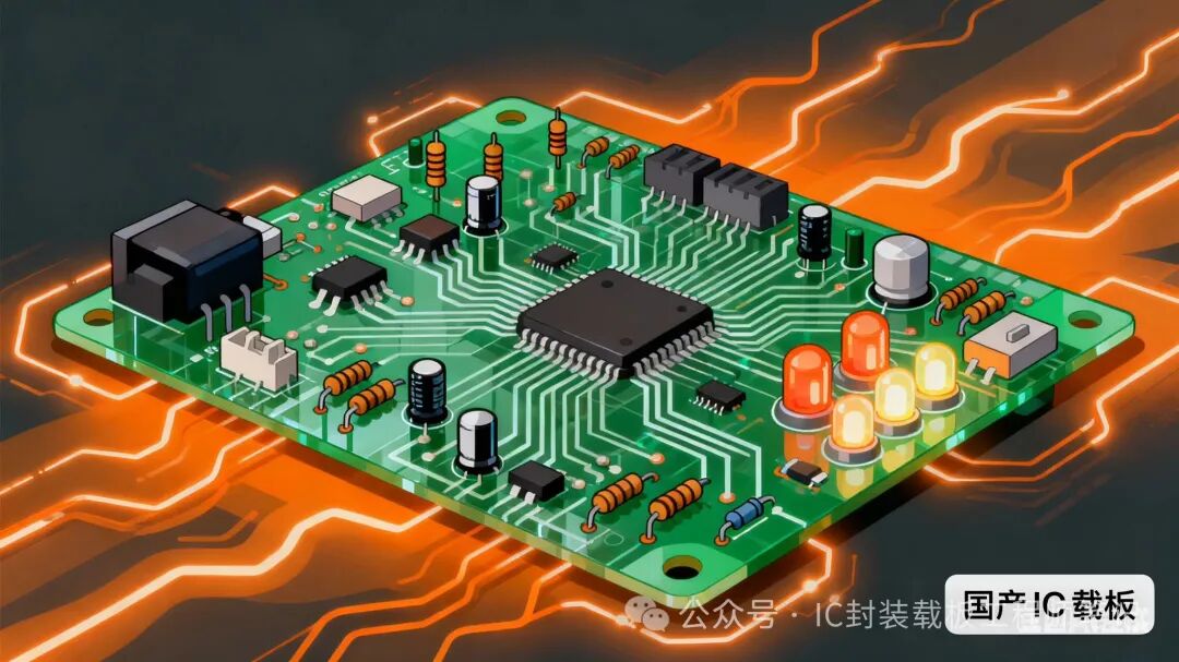
In the industrial control field, devices such as robots, CNC machine tools, and smart sensors require PCBs to provide real-time control and low-latency processing capabilities to ensure precise operation of the system.
4.3 New Requirements for IC Substrates Due to Advanced Packaging Technologies
With the rapid development of advanced packaging technologies, IC substrates face unprecedented technical challenges and opportunities. CoWoS technology is TSMC’s core technology for 2.5D packaging, integrating multiple chips through a silicon interposer, significantly enhancing bandwidth and energy efficiency using micro-bumps and silicon vias for high-density interconnections. CoWoS-S5 technology supports the high-density integration of 8 HBM3 memories and 2 SoC chips, breaking through to expand the interposer area to 2400mm², providing up to 5.3TB/s memory bandwidth for NVIDIA H100 GPUs, a threefold performance improvement over previous technologies. In terms of process precision, CoWoS-S5 employs hybrid bonding technology, reducing the bonding pitch to 1μm, achieving an astonishing I/O density of 1.2 million/mm², a 70-fold improvement over traditional micro-bump technology. HBM (high bandwidth memory) technology achieves over 1TB/s bandwidth per chip through 3D stacking and through-silicon via (TSV) technology, improving fivefold over traditional GDDR6. HBM requires advanced packaging technologies such as CoWoS, and its capacity is constrained by CoWoS capacity, leading to increased demand and supply shortages for CoWoS packaging.
4.4 Trends in Technology Evolution in the AI Era
AI and high-performance computing demands are reshaping the technological development direction of IC substrates and PCBs. In the IC substrate field, the technological development trends include: ultra-high density: line widths/spacing are developing from the current 10-15μm towards 5μm or even smaller, with a challenge to the 3μm technical limit by 2025. High layer counts: as chip integration increases, the layer count requirements for IC substrates continue to rise, with mainstream products currently being 14-20 layer structures, and the latest AI chip substrates expected to exceed 30 layers. New material applications: glass substrates are gaining attention as an emerging technology route, with advantages such as low dielectric constant (about 4.0) and low thermal expansion coefficient (about 3ppm/°C), closely matching silicon chips to reduce thermal stress. Intel plans to officially provide a complete glass substrate solution after 2025, aiming to achieve packaging of 1 trillion transistors before 2030. In the PCB field, technological development trends include: high frequency and high speed: applications in 5G communications and data centers are driving PCBs towards high frequency and high speed, raising higher requirements for dielectric constant and loss factor performance indicators. High multilayer counts: demand for multilayer boards with more than 18 layers is rapidly growing, with a growth rate of 40.3% expected in 2024, and the growth rate of these high-end categories is more than five times that of ordinary boards. System integration: HDI (high-density interconnect) technology has increased the wiring density of PCBs by more than 10 times per unit area, supporting the miniaturization of smartphones (for example, the motherboard area of the iPhone 15 is 60% smaller than that of the iPhone 4) and wearable devices (the mainboard of smartwatches is only the size of a fingernail).
5. Comprehensive Assessment of Costs and Supply Chains
5.1 Cost Structure Analysis of IC Substrates
IC substrates occupy a core position in the cost of electronic systems, with a distinct layered cost structure. In the composition of packaging costs, IC substrates account for about 30%, while substrate materials account for over 30% of the cost of IC substrates themselves, making the substrate material a key link in cost control. The specific cost composition includes: ABF film accounting for about 32% (the largest cost item), copper foil and substrate accounting for 8%, copper powder and gold salt accounting for 2%, and dry film accounting for 1.5%. In terms of application scenarios, the cost proportion of IC substrates varies significantly. In low-end packaging (WB type packaging), the cost of IC substrates accounts for 40-50% of material costs; in high-end packaging (FC type packaging), this proportion can reach 70-80%. This cost structure difference reflects the higher requirements for material performance, process complexity, and yield control in high-end IC substrates. Among the raw material costs of IC substrates, resin, copper foil, and copper balls are the three largest components, accounting for 35%, 8%, and 6%, respectively. Among these, ABF film, as a core material, has a price as high as 2000 yuan/square meter, which is six times that of ordinary BT resin. This high material cost directly drives up the overall manufacturing cost of IC substrates.
5.2 Cost Structure and Control Strategies of PCBs
The cost structure of PCBs is relatively transparent, with raw materials accounting for about 60%, among which copper-clad laminates are the largest cost item. The specific cost composition is as follows: copper-clad laminates account for 27.31%, prepreg accounts for 13.8%, labor costs account for 9.53%, gold salt accounts for 3.8%, copper balls account for 1.4%, copper foil accounts for 1.39%, dry film accounts for 1.37%, and ink accounts for 1.23%. In the cost composition of copper-clad laminates, copper foil accounts for 42.1%, glass fiber accounts for 26.1%, and epoxy resin accounts for 19.1%, meaning that price fluctuations in copper, glass fiber, and epoxy resin will directly impact PCB production costs. The cost control strategies for PCBs mainly include:
Material optimization: selecting appropriate substrate and copper foil thickness to balance performance and cost. For example, a 1.6mm thick board generally has a minimum hole diameter of 0.2mm, and costs will rise sharply for sizes smaller than 0.2mm, making processing very difficult. Process simplification: reducing unnecessary process steps, such as avoiding laser drilling or blind/buried holes, as these special processes significantly increase production costs. Mass production: reducing unit costs through batch production, as engineering design costs will be amortized as production volume increases.
5.3 Supply Chain Risk Assessment and Localization Progress
The supply chains of IC substrates and PCBs both face geopolitical risks and challenges of technological monopolies, but the degree of risk varies significantly between the two. In the IC substrate field, supply chain risks are extremely severe. Currently, the global IC substrate supply chain is highly concentrated in Asia, particularly in Japan, South Korea, and Taiwan. In 2023, the localization rate of substrate-specific equipment was only 26%, with key processes such as vacuum lamination and electroplating equipment still primarily relying on imports from Japan and Germany. More seriously, key materials such as ABF films are monopolized by Japanese companies, and any supply disruption would severely impact production. ABF substrates are almost entirely dependent on Japanese Ibiden, Shinko Electric, and South Korea’s Samsung Electro-Mechanics for supply, with domestic self-sufficiency approaching zero in 2024. In the PCB field, supply chain risks are relatively controllable, but high-end materials still rely on imports. Advanced packaging materials such as BT/ABF substrates have a global shortfall of over 30%, long controlled by Japan’s Mitsubishi Gas Chemical and Taiwan’s Nanya. Between 2022 and 2024, companies like Huawei and ZTE faced “supply disruptions” due to high-end copper-clad laminates, forcing delays in 5G base station delivery plans, exposing risks to industrial security. In terms of localization progress, Chinese companies are accelerating breakthroughs in key technological bottlenecks: in the materials field, Defu Technology plans to acquire Doosan’s copper foil business in Luxembourg, and HVLP3 generation copper foil has been supplied in batches for AI servers; Cuprum’s HVLP2 generation shipments account for over 60%, with HVLP4 generation capacity utilization reaching 85%; Longyang Electronics’ HVLP5 generation is entering customer validation, with mass production expected by the end of 2025. In the equipment field, Samsung Electronics’ exports of semiconductor equipment to China are expected to grow by 60% in 2024, while SK Hynix’s related business is expected to grow by 45%, while Japan’s semiconductor equipment global sales are only expected to grow by 1%. This indicates that Chinese companies are actively expanding alternative sources to reduce dependence on Japanese equipment.
5.4 Cost Control and Supply Chain Optimization Strategies
In the face of complex cost structures and supply chain risks, companies need to adopt diversified optimization strategies: technological innovation to reduce costs: through process innovation to reduce material consumption and improve yield. For example, the mSAP process can reduce packaging costs by over 30% compared to traditional subtractive methods. Supply chain diversification: actively expanding sources of materials and equipment to reduce dependence on single suppliers. Chinese companies are turning to suppliers in South America, such as Argentina, for photoresists while increasing procurement of equipment from South Korea. Localization substitution: increasing R&D investment to break through key material and equipment technological bottlenecks. Xingsen Technology has been engaged in packaging substrate business since 2012, achieving mass production of ABF substrates only by the end of 2024, which fully illustrates the difficulty and importance of technological breakthroughs. Industry collaboration: achieving technological sharing and risk-sharing through cooperation between upstream and downstream in the industry chain. For example, Taiwanese companies have formed a complete industry chain from wafer foundry to packaging testing, with TSMC or UMC for foundry, ASE and SPIL for packaging, and Kingboard providing substrates, greatly improving efficiency and competitiveness.
6. Decision Framework: Guidelines for Choosing IC Substrates and PCBs
6.1 Decision Factors for Technology Selection
When choosing between IC substrates and PCBs, it is essential to consider multiple key factors such as performance requirements, cost constraints, application scenarios, and technological maturity. Performance requirement-driven selection principle: If the application scenario has strict requirements for ultra-high-density interconnections, such as in high-performance computing scenarios involving CPUs, GPUs, and AI chips, IC substrates are the inevitable choice. IC substrates feature high density, high precision, high performance, miniaturization, and thinness, with line widths/spacing reaching 5-20μm, meeting the needs for interconnections of micro-sized chip pins. Particularly in AI servers and data centers, IC substrates are critical for packaging high-performance chips. If the application scenario emphasizes system integration and cost-effectiveness, such as in consumer electronics, automotive electronics, and industrial control, PCBs are the more suitable choice. PCBs can connect and support various types of electronic components, forming complex circuit systems, and their manufacturing costs are relatively low, making them suitable for mass production.
Cost constraint-based selection strategy: From a cost perspective, the cost of IC substrates is typically several times or even tens of times that of PCBs. IC substrates account for 40-50% of costs in low-end packaging and 70-80% in high-end packaging. Therefore, in cost-sensitive applications, PCB solutions should be prioritized. However, it is important to note that in certain high-end applications, although the unit price of IC substrates is higher, the system advantages brought by their high performance may lead to overall cost reductions. For example, in AI servers, using high-performance chips packaged with IC substrates can significantly enhance computing efficiency and reduce system power consumption, potentially offering advantages from a total lifecycle cost perspective. Application scenario adaptability analysis: IC substrates are mainly suitable for the following scenarios: • High-performance computing: CPUs, GPUs, AI chips, etc. • High bandwidth storage: HBM, high-speed caches, etc. • High-frequency communications: 5G/6G RF chips, high-speed interfaces, etc. • Special requirements: applications with strict requirements for size, weight, and power consumption. PCBs are mainly suitable for the following scenarios: • Consumer electronics: smartphones, computers, home appliances, etc. • Automotive electronics: in-vehicle systems, new energy vehicles, etc. • Industrial control: robots, automation equipment, etc. • Communication equipment: base stations, switches, routers, etc.
6.2 Typical Application Case Analysis
Through specific cases, the selection logic between IC substrates and PCBs can be better understood: Case 1: Smartphone Chip System
In smartphones, IC substrates carry the most critical chips: • AP (application processor): such as Snapdragon 8 Gen series, Apple A series, using ABF or BT substrates to achieve high-density interconnections between SoCs and external circuits. • Storage chips: LPDDR memory, UFS flash memory, using CSP substrates for miniaturized packaging. • RF chips: 5G baseband, RF front-end modules, using high-frequency substrates to meet the high-performance requirements of 5G communications. PCBs provide system-level connections: • Motherboard: using HDI PCBs with more than 10 layers, integrating all components such as CPU, memory, RF, and sensors. • Flexible boards: connecting components such as displays, cameras, and batteries for flexible interconnections. • Special function boards: such as wireless charging coils, antenna modules, etc. This combination fully leverages the ultra-high-density interconnection advantages of IC substrates and the system integration capabilities of PCBs. Case 2: AI Server System
In AI servers, the role of IC substrates is even more critical: • GPU chips: such as NVIDIA H100, B200, using 2.5D packaging substrates to integrate multiple chips and HBM memory. • CPU chips: such as Intel Xeon, AMD EPYC, using high-end ABF substrates to support ultra-multi-core and high-speed interconnections. • High-speed interfaces: such as InfiniBand, PCIe 5.0, using high-frequency substrates to ensure low-latency data transmission. PCBs provide infrastructure: • Motherboard: using high multilayer PCBs with more than 20 layers, carrying CPU, GPU, memory, network chips, etc. • Backplane: used to connect multiple motherboards, providing high-speed interconnection channels. • Power board: providing stable power supply, using thick copper PCB designs. Case 3: New Energy Vehicle Electronic Systems
New energy vehicles have high requirements for electronic systems, necessitating the collaborative use of IC substrates and PCBs: IC substrate applications: • Power semiconductors: IGBT modules using ceramic substrates to meet high power and high reliability requirements. • In-vehicle chips: autonomous driving chips, in-car chips using high-end substrates. • Sensors: MEMS sensors using miniaturized substrates. PCB applications: • Battery management systems (BMS): using multilayer PCBs to monitor battery status. • Electronic control systems (ECU): using high-reliability PCBs to meet automotive-grade standards. • In-vehicle networks: using high-speed PCBs to achieve in-vehicle network communication.
6.3 Impact of Technological Development Trends on Selection
With the rapid development of technology, the boundaries between IC substrates and PCBs are changing, which has significant implications for selection decisions: Technological integration trend: • High-end PCBs are approaching the technical specifications of IC substrates, with HDI technology enabling PCB line widths/spacing to reach 15-20μm. • IC substrate technology is also evolving towards larger sizes and higher layer counts to meet system integration needs. • New types of substrate technologies that integrate IC substrates and PCBs may emerge in the future. Evolving application demands: • AI and edge computing are driving the demand for integrated solutions of “chip + substrate + PCB.” • 5G/6G communications require higher integration and lower latency. • New energy vehicles require more reliable and efficient electronic systems. Cost-effectiveness considerations: • With technological advancements and mass production, the costs of IC substrates are decreasing. • However, monopolies on key materials and equipment may drive up long-term costs. • It is necessary to comprehensively consider technical performance, supply security, and total lifecycle costs.
6.4 Risk Assessment and Response Strategies
When choosing between IC substrates and PCBs, it is also essential to fully assess potential risks and develop response strategies: Technical risks: • IC substrates: high technical barriers, difficult yield control, with yields for substrates over 10 layers only at 30%-50%. • PCBs: facing signal integrity challenges in high-frequency and high-speed applications. Response strategies: strengthen R&D investment, establish long-term partnerships with suppliers, and develop technical backup plans. Supply chain risks: • IC substrates: severe reliance on imports for key materials (such as ABF films) and equipment. • PCBs: high-end materials and equipment also have import dependencies. Response strategies: promote localization substitution, expand supply channels, and establish strategic inventories. Cost risks: • IC substrates: high material costs and significant price fluctuations. • PCBs: affected by prices of raw materials such as copper. Response strategies: use long-term contracts to lock in prices, develop alternative materials, and optimize designs to reduce material consumption. Market risks: • Rapid technological iterations and shortened product lifecycles. • Changes in customer demand may lead to inventory backlogs. Response strategies: maintain technological sensitivity, establish flexible production systems, and enhance market forecasting.
Conclusion
IC substrates and PCBs, as the twin stars of the electronics industry, exhibit significant differences in technical characteristics, application scenarios, and market landscapes, while also showing deep integration trends. Through this in-depth analysis, the following key conclusions can be drawn: On a technical level, IC substrates represent the highest standard of interconnection technology, with line widths/spacing breaking through 5μm and moving towards 3μm, while PCBs have advantages in system integration and cost control. The differences in material systems, manufacturing processes, and performance indicators between the two determine their different positioning and value in electronic systems. In terms of market landscape, the global IC substrate market exhibits a highly monopolized characteristic, dominated by companies from Japan, South Korea, and Taiwan, while the PCB market is relatively dispersed, with Chinese companies occupying an important position. However, the localization rate in the high-end product field remains low, especially for ABF substrates, which are almost entirely reliant on imports. In terms of application trends, the demand for AI and high-performance computing is reshaping the industry landscape, driving IC substrates towards ultra-high density, high layer counts, and new materials, while also boosting the demand for high-end PCBs. Advanced packaging technologies such as CoWoS and Chiplet present unprecedented challenges and opportunities for substrates. In terms of supply chain security, the reliance on imports for key materials and equipment poses the greatest risk, particularly the monopolistic position of Japanese companies in core materials such as ABF films. Chinese companies need to increase R&D investment, promote localization substitution, and establish a secure and controllable supply chain system. Looking ahead, as electronic technology advances towards higher performance, smaller sizes, and lower power consumption, both IC substrates and PCBs will face new opportunities and challenges. For industry participants, it is essential to accurately grasp technological development trends and formulate differentiated development strategies: Recommendations for enterprises: • IC substrate companies should focus on technological breakthroughs, particularly achieving autonomy and control in key areas such as ABF materials and high-end equipment. • PCB companies should upgrade towards high-end and intelligent directions, enhancing competitiveness in high-frequency, high-speed, and high-multilayer board fields. • Strengthen industry chain collaboration to achieve technological sharing and risk-sharing through cooperation between upstream and downstream. Recommendations for investors: • Focus on companies with core technological breakthrough capabilities, especially in key areas such as materials and equipment. • Pay attention to market opportunities brought by downstream applications such as AI and new energy vehicles. • Assess supply chain risks and choose investment targets with autonomous control capabilities. Recommendations for policymakers: • Increase support for key technology R&D, particularly in foundational areas such as materials and equipment. • Promote collaborative innovation in the industry, establishing an integrated innovation system of production, learning, research, and application. • Improve industrial policies to support localization substitution and ensure the security of the industrial chain and supply chain. The technological competition and integrated development of IC substrates and PCBs not only drive the progress of the electronics industry but also relate to national technological competitiveness and industrial security. In this critical period of technological transformation, only by accurately grasping technological trends and strengthening independent innovation can we occupy a favorable position in global competition and lay a solid foundation for the high-quality development of China’s electronics industry.