This article takes the Cortex-A53 processor as an example, accessing the internal storage units (tag RAM and dirty RAM) in the processor to read the MOESI information in the cache line.
The Cortex-A53 provides a mechanism to access some internal storage units used by the Cache and TLB by reading certain system registers. This feature can probe issues that arise when the data in the cache is inconsistent with the data in main memory.
Additionally, the reading methods differ between A64 mode and A32 mode:
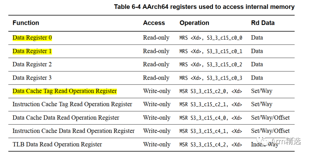
When the processor is in A64 mode, it first selects the specific cache line and memory address through some write-only registers, and then reads the specific tag information through read-only registers. The following diagram shows the relevant registers and operation instructions. It should be noted that these operations are only available in EL3; using these instructions in other modes will result in an Undefined Instruction exception.
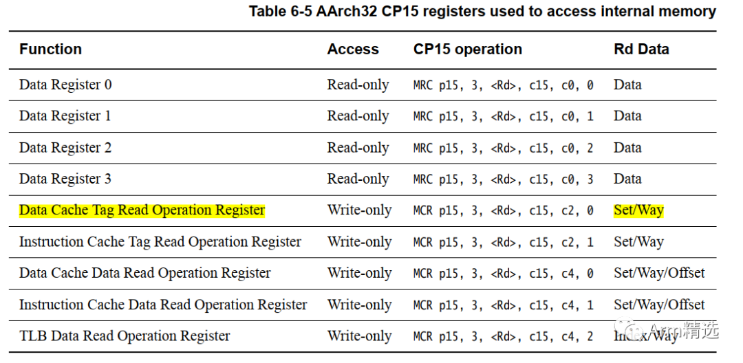
When the processor is in A32 mode, it first selects the specific cache line and memory address through some write-only CP15 registers, and then reads the specific tag information through read-only CP15 registers. The following diagram shows the relevant registers and operation instructions. It should be noted that these operations are only available in EL3; using these CP15 instructions in other modes will result in an Undefined Instruction exception.
Next, this article takes the Data cache of Cortex-A53 as an example to read the tag information of a specific cache line. The specific steps are simple and consist of two parts:
- Write to the Data Cache Tag Read Operation Register, with the content being the specific Set and way information, to locate the desired cache line using the way index and set index.
- Read the corresponding Data Register 0 and Data Register 1 registers. By decoding the data inside the Data Register registers, we can obtain the tag information. Other information, such as the data information of the Data cache, the data or tag information of the Instruction Cache, and the data information of the TLB, can all be read in this way.
Step 1: Write Set/way Information to Data Cache Tag Read Operation Register
First, we need to parse the Set index information from a virtual address (VA).
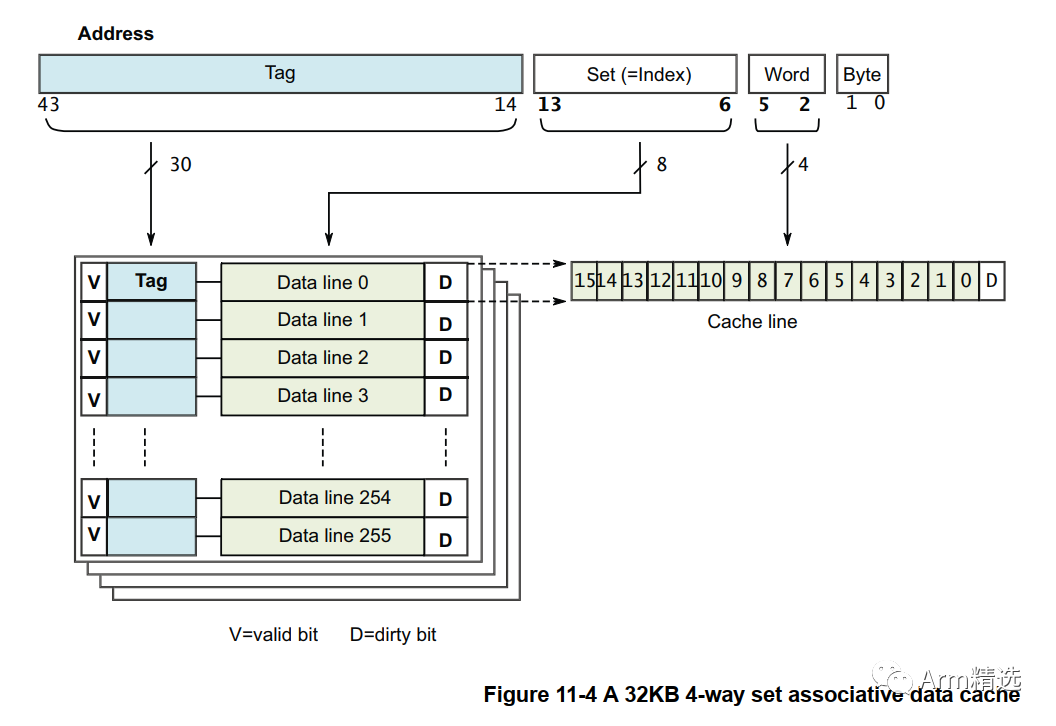
The following diagram shows the structure of the 32KB data cache of Cortex-A57, which is 4-way set associative, with a cache line size of 64 bytes. From the diagram, we can see that a VA can be divided into several parts: Tag, Set index, word index, and byte index. Among them, Set index = VA[13:6].
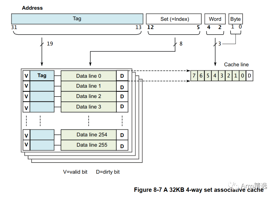
In another example, for a 32KB 4-way set associative data cache with a cache line size of 32 bytes, its Set index = VA[12:5]:
The Data cache of Cortex-A53 is a 4-way set associative structure. Assuming it is 32KB and the size of a cache line is 64 bytes, we can calculate that there are 32 KB / 64 B / 4 = 2^7 = 128 sets in this data cache, which means at least 7 bits are needed to fully parse the specific set index. As shown in the following formula:
S = log2(Data cache size / 4).to calculate the range of Set index: Set index = VA[12:6].
Since it is a 4-way set associative structure, the cache line can exist in any of the ways, so our cache way could be any number among 0, 1, 2, or 3.
After obtaining the set and way indices, they need to be encoded and then written into the Data Cache Tag Read Operation Register. The encoding rules are shown in the following diagram, where we simply write the values of Set and way into the corresponding bits, and Rd[5:3] is the offset of the cache double word data. Since this example is reading tag information, Rd[5:3] can be set to 0.
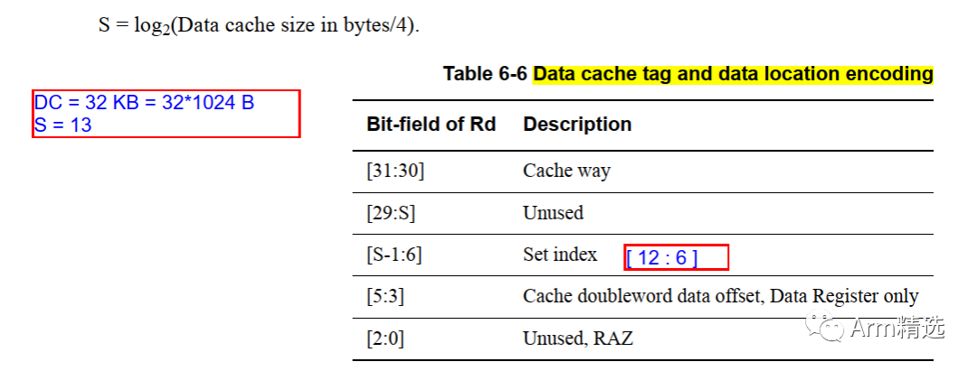
Thus, the value we need to write into the Data Cache Tag Read Operation Register for Rd can be obtained through the following code:
unsigned int get_Rd_data(int * VA, way_num){ unsigned int set_way_index = VA | 0x1FC0; //get way index, VA[12:6] set_way_index |= way_num < 30; //way_num could be 0,1,2,3 return set_way_index;}In Rd, besides the Set and way information, all other values are 0, and 0x1FC0 represents the case where VA[12:6] is all 1s:
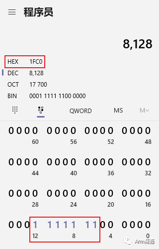
Then we use the CP15 register to write the value of Rd, assuming Rd is R0:
MCR p15, 3, r0, c15, c2, 0 ; r0 = get_Rd_data(VA,way_num)Step 2: Read Data Register 1 and Data Register 0 Data and Decode
After writing the Set/way information into the Data Cache Tag Read Operation Register, it is equivalent to selecting the cache line to operate on. Next, we will read the data from Data Register 1 and Data Register 0 to obtain the tag information from that cache line. Besides the tag information, we can also obtain the following from Data Register 1 and Data Register 0:
- MOESI state information
- Outer memory attributes
- Valid information
The specific information that can be obtained is shown in the following diagram:
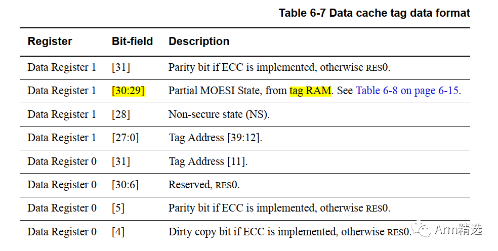
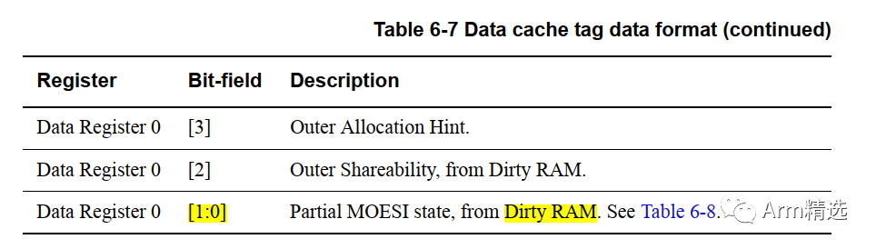
It should be noted that if you want to obtain the MOESI state information, you need to use two registers in conjunction, that is, read Data Register 0 [1:0] and Data Register 1 [30:29]. The Data Register 0 [1:0] contains the part of the state information from the Dirty RAM, while Data Register 1 [30:29] contains the part of the MOESI information from the tag RAM.
The specific combination is shown in the following diagram:
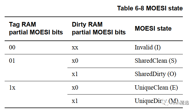
For example, if the read values of Data Register 0 [1:0] are 1, and Data Register 1 [30:29] is also 1, based on the combination relationship shown above, we can conclude that the current cache line’s MOESI state is SharedDirty (O).
Sample code is as follows:
; step 1: write set index and way num into Data Cache Tag Read Operation RegisterMCR p15, 3, r0, c15, c2, 0 ; r0 = get_Rd_data(VA,way_num); step 2: read Data Register 1 and Data Register 0MCR p15, 3, r1, c15, c0, 0 ;r1 = Data Register 0 MCR p15, 3, r2, c15, c0, 1 ;r2 = Data Register 1This article is reprinted from CSDN, author: SOC Luo Sanpao, the article has obtained the copyright of the original author.