
Printed circuit boards (PCBs) are widely used in various electronic devices, whether in mobile phones, computers, or complex machinery, you can find circuit boards. If there are defects or manufacturing issues with the PCB or PCBA, it may lead to failures in the final product and cause inconvenience. In such cases, manufacturers will have to recall these devices and spend more time and resources to fix the issues.
Therefore, PCBA testing has become an indispensable part of the circuit board manufacturing process, as it detects issues in a timely manner, assists staff in quick handling, and ensures high quality of PCBA.
Let’s explore the 14 common testing methods for PCBs.
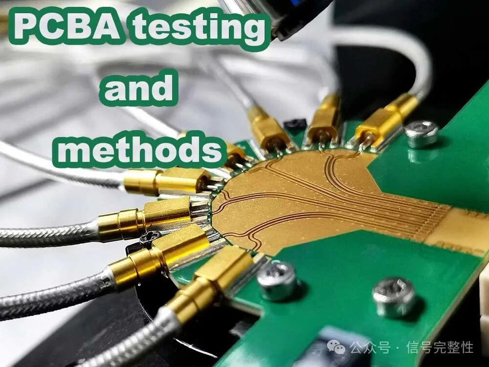
1. In-Circuit Testing (ICT)
ICT, or Automated In-Circuit Testing, is essential testing equipment for modern PCB manufacturers and is very powerful. It primarily detects open circuits, short circuits, and faults in all components by having test probes contact the test points laid out on the PCB, clearly informing the staff of the results.
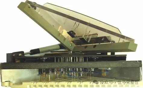
ICT has a wide range of applications, high measurement accuracy, and clear indications of detected issues, making it very easy for workers with average electronic technology skills to handle problematic PCBAs. Using ICT can greatly improve production efficiency and reduce production costs.
2. Flying Probe Testing
Flying probe testing, like ICT, is a recognized effective testing method that can effectively identify production quality issues. However, flying probe testing has proven to be a particularly cost-effective method for improving circuit board standards.
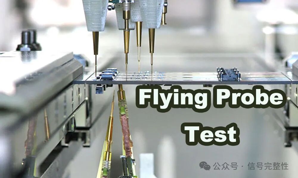
Unlike traditional testing methods that use fixed-position test probes, flying probe testing employs two or more independent probes that operate without fixed test points. These probes are electromechanically controlled and move according to specific software instructions. Therefore, the initial cost of flying probe testing is lower, as it can be completed by modifying software without changing fixed structures. In contrast, ICT has a higher initial fixture cost, making flying probe testing cheaper for small batch orders, while ICT is faster and less error-prone, making it more cost-effective for large batch orders.
3. Functional Testing
Functional system testing uses dedicated testing equipment at the middle and end of the production line to comprehensively test the functional modules of the circuit board to confirm its quality. Functional testing mainly includes Final Product Testing and Hot Mock-up.
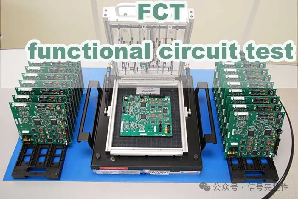
Functional testing typically does not provide in-depth data (e.g., pin positions and component-level diagnostics) to improve processes, and requires specialized equipment and specially designed testing programs. Writing functional testing programs is very complex, making it unsuitable for most circuit board production lines.
4. Automated Optical Inspection (AOI)
AOI uses a single 2D camera or two 3D cameras to take photos of the PCB and then compares the images with detailed schematics. If the PCB does not match the schematics to a certain extent, the mismatched areas are flagged for technician inspection, allowing AOI to detect faults in a timely manner.
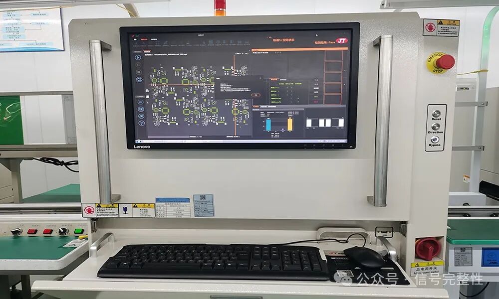
However, AOI testing does not power the PCB and cannot detect 100% of all component issues, so AOI is generally used in conjunction with other testing methods. Common testing combinations include:
● AOI and Flying Probe
● AOI and In-Circuit Testing (ICT)
● AOI and Functional Testing
5. X-ray Testing
X-ray testing, or X-ray inspection, uses low-energy X-rays to quickly detect issues such as open circuits, short circuits, cold solder joints, and solder leaks on the circuit board.
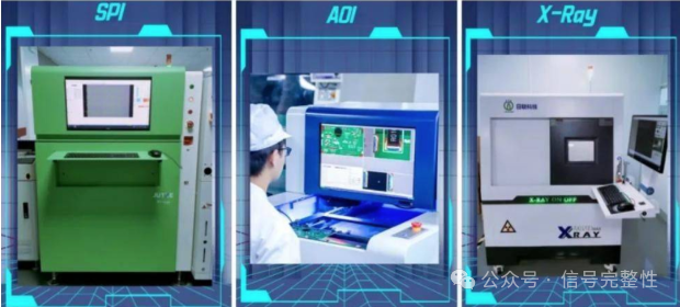
Image source: Huaqiu Circuit
X-ray is mainly used to detect defects in ultra-fine pitch and ultra-high density circuit boards, as well as defects such as bridging, missing chips, and misalignment that occur during assembly. It can also use tomography to detect internal defects in IC chips. This is the only method to test the quality of BGA solder and ball bonding. The main advantage is that it can check BGA solder quality and embedded components without the need for fixed fixtures.
6. Laser Testing
This is the latest development in PCB testing technology. It uses a laser beam to scan the printed board, collecting all measurement data and comparing the actual measurements with preset acceptance limits. This technology has been validated on bare boards and is being considered for assembly board testing. The speed is sufficient for mass production lines. Its main advantages are fast output, no fixtures, and clear visibility; its main disadvantages are high initial costs and maintenance and usage issues.
7. Aging Testing
Aging testing refers to the process of simulating various factors involved in the real use conditions of the product to conduct corresponding condition-enhanced experiments. The purpose is to test the stability and reliability of the product under specific environmental conditions.
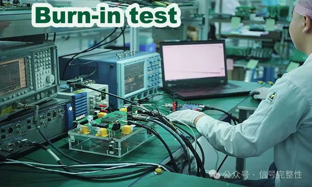
According to design requirements, the product is placed under specific temperature and humidity conditions, simulating operation for 72 hours to 7 days, recording performance data, and backtracking the production process for improvements to ensure its performance meets market demands. Aging testing typically refers to electrical performance testing, with similar tests including drop testing, vibration testing, and salt spray testing.
8. Solderability Testing
Ensures a solid surface and increases the chances of forming reliable solder joints. Solderability testing refers to the assessment of the soldering performance of components, PCB boards, pads, solder, and flux through the wetting balance method.
9. PCB Contamination Testing
PCB ion contamination refers to the residual ionic contaminants on the PCBA surface from flux residues, chemical cleaning agents, humidity, electroplating, wave soldering, reflow soldering, and other processes. PCN contamination detection can identify a large number of ions that may contaminate the circuit board, leading to corrosion and other issues.
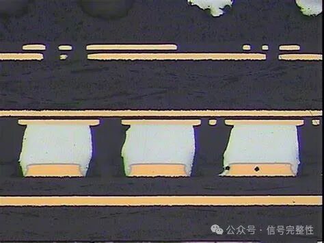
10. Cross-Sectional Analysis
Investigates defects, open circuits, short circuits, and other failures.
11. TDR Testing
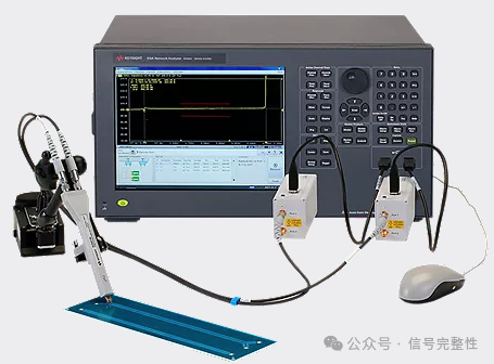
When discovering faults in high-speed or high-frequency boards, it is recommended to use TDR for testing analysis, which can quickly determine whether there are open or short circuits and identify the location of the faults.
12. Peel Testing
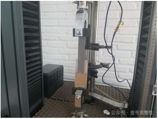
PCB peel strength testing generally refers to the bond strength testing between copper foil and substrate or between copper foil and brown film. It assesses the bonding strength between PCB copper foil and substrate after receiving conditions, thermal stress, and high-temperature conditions.
13. Float Solder Testing
Determines the level of thermal stress that PCB holes can withstand. This test is applicable to plated holes, surface conductors, and pads. Before testing, the surface of the solder should be thoroughly cleaned of dross and flux residues. The sample is then floated on molten solder for a maximum of 5 minutes, ensuring that the immersion depth does not exceed 50% of the sample thickness. After the dwell time, the sample is removed from the solder and kept level until the solder solidifies.
14. Wave Solder Testing
This test is applicable to plated holes, surface conductors, and pads for wave soldering. Relevant parameters are set and recorded: clamping method (if required), transfer speed, preheating, soldering device with or without anti-oxidation oil, equipment process control, tilt angle, board preheating temperature, and soldering temperature.
PCBA testing is an essential part of ensuring product delivery quality. It determines product performance, controls product quality, and reduces after-sales and repair rates.

Some Screenshots from Electronic Books
【Complete Set of Hardware Learning Materials Collection】