Chips are hidden in theelectronic devices that can be seen everywhere in cities, and smartphones, computers, and home appliances all rely on their control.
The tiny chipintegrates a vast scale of circuits.
When magnifying the chip, you can see that its interior is filled with densely packed circuit layouts, resembling a tightly woven highway, as if a well-organized circuit city has been built in an extremely small size.
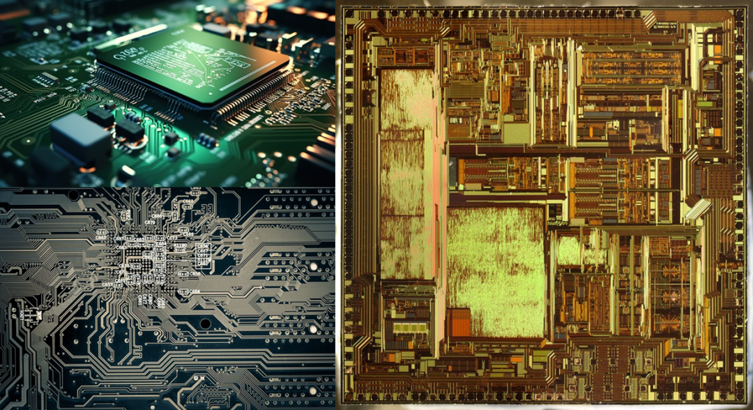
Chip structure diagram (naked eye and microscopic) | Image source: pixabay
How small is the interior of a chip? Currently, the smallest process used in industrial chips, which is thesmallest size humans can create, has reached 3nm, allowing the chip to integrate over tens of billions of transistors.
The “Multi-layer” Approach to Chip Manufacturing
Are countless nanoscale electronic components arranged on the chip pre-made and placed one by one?
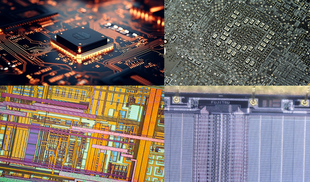
Image source: pixabay (top); Searchmedia – Wikimedia Commons (bottom)
No! We can look at this problem from a different angle. Upon careful observation from a vertical perspective, we can find that the chip is made up oflayered structures with different patterns stacked vertically. If we pre-make each layer and then stack them vertically, the two-dimensional structures can combine to form a three-dimensional device, ultimately resulting in a functionally rich chip.
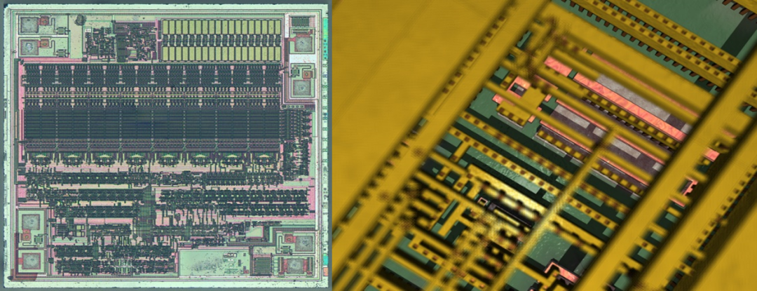
Vertical observation of the internal structure of the chip | Image source: Searchmedia – Wikimedia Commons
Now our goal becomes how to create a layered structure with specific patterns. First, we need asheet material to print the circuit diagram, which is thesilicon wafer we often hear about. This is a highly pure silicon that is processed and cut into smooth, extremely thin disks.
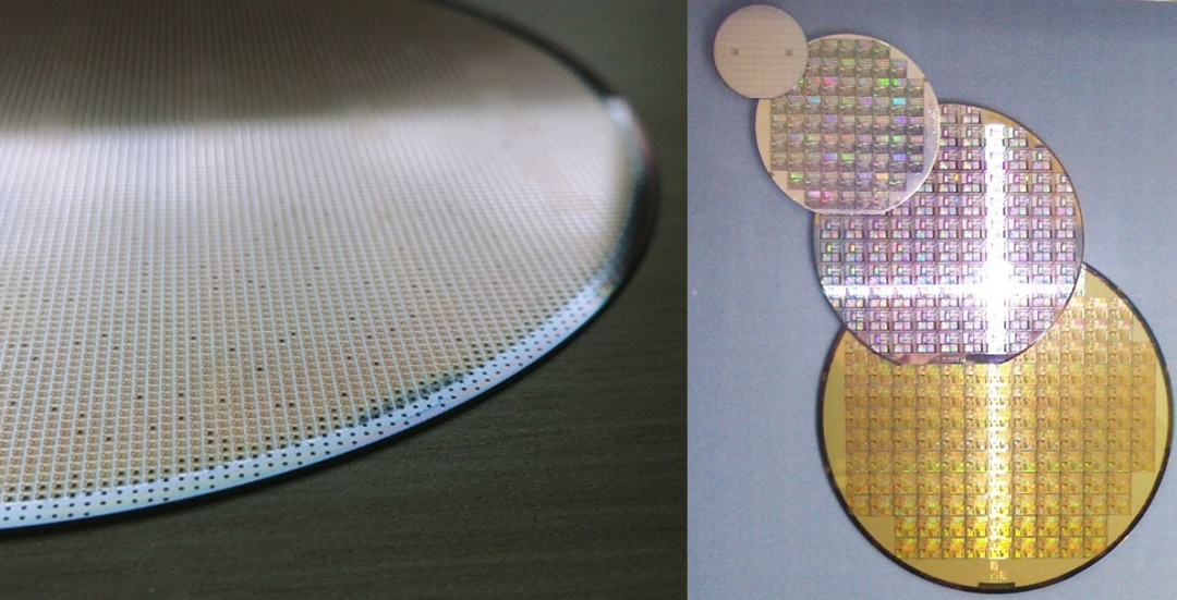
Silicon wafer | Image source: pixabay (left); Searchmedia – Wikimedia Commons (right)
Next, just like a carpenter, we need to find the right tools to carve patterns. To create a chip with a complex internal structure that is extremely small, thesize of the processing tools must be extremely precise.
We clever humans have found that light can serve as this carving knife. Because light hasrich wavelengths, we canuse short wavelengths of light to achieve extremely fine processing.
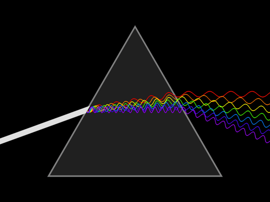
The rich wavelengths of visible light (invisible light has even richer wavelengths) | Image source: Searchmedia – Wikimedia Commons
We hope to transfer the circuit patterns designed on paper to the silicon wafer throughoptical exposure, but light cannot affect silicon materials, so we need an intermediate material that can directly interact with light, which isphotoresist.

Photoresist spun onto the silicon wafer (evenly covered by centrifugal force) | Image source: Searchmedia – Wikimedia Commons
To allow light totransmit the pattern information, we can use a method that completely blocks or completely allows light to pass through to create a light and dark pattern. Light passes througha mask with a circuit pattern, which canreplicate the pattern information of the mask. Finally, after interacting with the photoresist evenly covering the surface of the silicon wafer, the required pattern information appears on the silicon wafer.
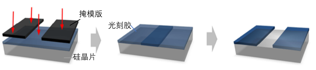
Photolithography imaging exposure process | Image source: Searchmedia – Wikimedia Commons
Photoresist is themain medium for photolithographic imaging, divided into positive and negative resists. The positive photoresist is more easily dissolved in thedeveloper in the exposed area, while the negative photoresist is less likely to dissolve in the developer.
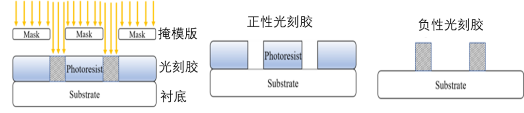
Two results of the exposure process (positive and negative resists) | Image source: Searchmedia – Wikimedia Commons
Assuming that positive photoresist is used, after the exposure process, the developer can dissolve the exposed photoresist. Then, usingchemical substances to dissolve the exposed silicon wafer, the photoresist remaining on the surface of the silicon wafer protects it, which is theetching process.
Now we have achieved our goal, obtaining a silicon wafer with a specific circuit pattern. Throughout this process, the general idea is relatively smooth, but the precision engineering of chip manufacturing, representing the pinnacle of human wisdom, involves countless strict requirements.
What Limits the Size of Chip Interiors?
The main component of a chip is the transistor, and a large chip can have over tens of billions of transistors. The smaller we can manufacture transistors, the morecomponents the chip can accommodate, and thepower consumption of the transistors will also be lower.
In chip manufacturing, we hope to uselight to create circuit patterns at small scales. So why can light achieve this effect? What are the limits of light’s engraving?
1
Diffraction
The main reason affecting the engraving level of light is thediffraction effect of light. Light is an electromagnetic wave, and diffraction is inevitable during the propagation of light in photolithography, resulting in a minimum feature size in the exposure range. The resolution of light, which is the ability of the photoresist to reconstruct patterns based on light exposure, is also limited.
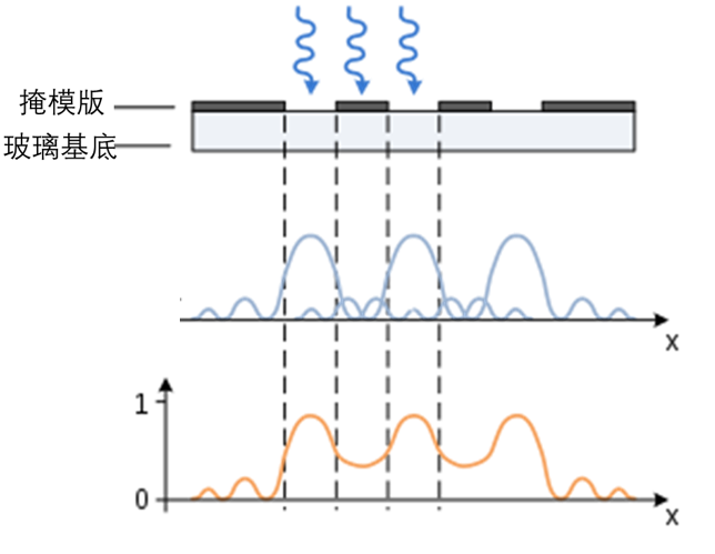
Diffraction during the exposure process | Image source: Searchmedia – Wikimedia Commons
As shown in the figure, when a beam of parallel light passes through a narrow slit, the light will interfere with itself in countless sub-waves during propagation, forming an alternating diffraction pattern.
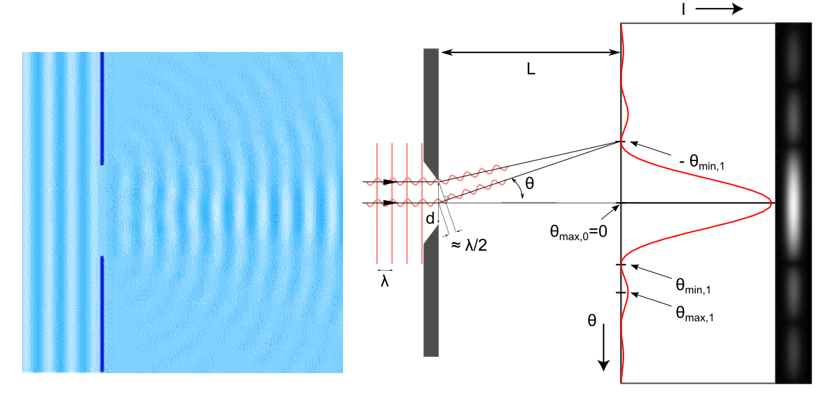
Single-slit diffraction | Image source: Searchmedia – Wikimedia Commons
This means that when considering the propagation of light at a small scale, the light areas are no longer distinctly separated from the non-light areas, but ratherthere are blurred zones. An ideal point of light emitted from an object will deviate from the geometric optical straight line after passing the edge of an obstacle, no longer forming an ideal image point.
This is precisely because whenthe width of the slit is comparable to the wavelength of light, the wave effects of light come into play, allowing light to usewave effects to bypass obstacles anddiffuse in space, resulting in the diffraction effect of light, causing theexposure area to lose precision, and the resolution of light has limits.
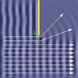
Light wave effect diagram (comparing straight propagation and wave effects) | Image source: Searchmedia – Wikimedia Commons
2
Resolution
In the field of optical imaging,resolution is the ability to distinguish between two adjacent points. Ideally, we want each point to producea sharp image point, but due to diffraction, the actual result islight spots of a certain size. If two light spots (diffraction patterns)overlap too much, the image points are difficult to distinguish.
Rayleigh proposed an effective criterion, and the resolution calculation formula is:
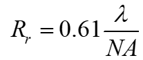
This resolution expression describes the limit position at which two light spots can just be distinguished—when the maximum position of one light spot coincides with the first zero point of the other. Here, λ is the wavelength of the illuminating light.
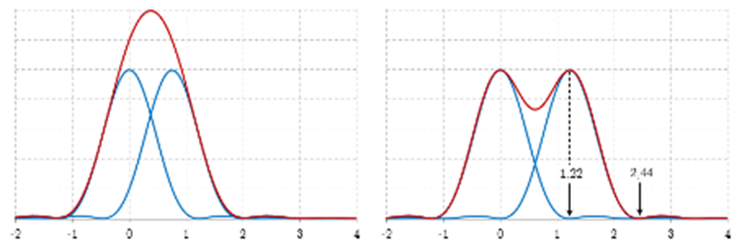
The limit situations of indistinguishable and just distinguishable light spots | Image source: Searchmedia – Wikimedia Commons
NA is the numerical aperture, which describes thelight gathering ability of the lens, specifically manifested in the degree of deflection of parallel light upon incidence (converging to a focal point), calculated as:
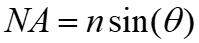
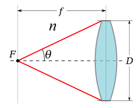
Numerical aperture (n is the refractive index) | Image source: Searchmedia – Wikimedia Commons
The Rayleigh criterion is commonly used to evaluate imaging quality, while the photolithography system images in photoresist.Photoresist is a high-contrast imaging medium, and under certain exposure conditions, although the optical resolution has reached below the Rayleigh criterion limit, the photoresistcan still present good imaging results, achieving processing goals.
The resolution of photolithographic imaging is:
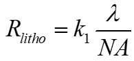
Rlitho is the resolvable pattern period of the photolithography system; k1 is the process factor.
3
Photolithography
Photolithography is the most complex, expensive, and critical process in chip manufacturing, usually using a projection photolithography system toproject the circuit structure diagram of the mask onto the surface of the silicon wafer.
Optical lenses canfocus diffracted light to improve imaging quality, and in lithography technology, to achieve the smallest possible patterns, a projection imaging objective with areduction ratio is used between the mask and the photoresist.
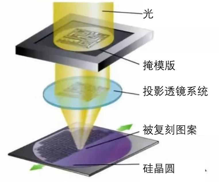
Projection photolithography system | Image source: the internet
How to Polish the Carving Knife of Light?
We now know that:the minimum processing scale of light (resolution) determines how small the chip can be. How can we make the chip smaller? We need toenhance the resolution capability and refine the functions of the circuit city on the chip.
Based on the three factors in the photolithography resolution formula, we have three solutions to polish the carving knife of light.
· Increase the numerical aperture of the lithography system
The larger the numerical aperture of the projection lens in the lithography imaging system, the better the resolution capability. Specifically, this is achieved by designingimmersion lithography machines, which fill a high refractive index medium between the wafer and the last lens of the projection lens.
· Shorten the wavelength
The light wavelengths used in the lithography process have undergone a development history from G-line (432nm), I-line (365nm), KrF (248nm), to ArF (193nm). Currently, extreme ultraviolet lithography (EUV) with a wavelength of 13.5nm has been put into use.
· Reduce the process factor
Byoptimizing lithography process parameters, we can also improve lithography resolution, such as improving lighting conditions, photoresist processes, and mask design. These methods can reduce the process factor k1, known as resolution enhancement technology (RET).
Light isan electromagnetic wave, thus containing information such asamplitude, phase, polarization state, and propagation direction. Resolution enhancement technology in photolithography adjusts these four aspects of light to achieve finer graphic structures on photoresist. For example, off-axis illumination technology can change amplitude and phase, optical proximity effect correction technology can change the amplitude of light waves, and source-mask optimization can change the propagation direction, amplitude, and phase of light waves.
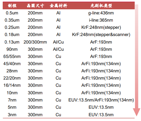
Relationship between various process nodes and lithography technology | Source: Sacom Microelectronics official website, ASML, Zhongtai Securities Research Institute
Looking at the development history of lithography machines, we are indeed running along the path of continuously shortening wavelengths. Observing the data in the table, whenthe wavelength of the light source remains the same, we are still continuously minimizing the process, thanks to the numerical aperture, process factor, and other complex technologies.
References
[1] Wei Yayi. Calculation of Lithography and Layout Optimization [M]. 1. Electronics Industry Press, 2021.
[2] Stephen A. Campbell. Micro-nano Scale Manufacturing Engineering [M]. 3. Electronics Industry Press, 2010.
Planning and Production
Source丨Institute of Physics, Chinese Academy of Sciences
Editor丨Wang Mengru
Proofreader丨Xu Lai, Lin Lin

Related Articles

1. Does long-term 16+8 intermittent fasting increase mortality by 91%? Don’t be fooled!
2. Trapped in a “tin coffin” for over 70 years, living only by mouth… The longest surviving “iron lung patient” in the world has passed away.
3. A small habit while cooking can raise blood sugar and increase weight, better change it!
4. People who often eat these 4 types of food are most likely to gain belly fat! Try these actions to lose the big belly.
5. Because it couldn’t bloom, this plant exploded, growing into this strange shape! People: Edible! Tasty!

Light up “Looking”
Let’s learn together!