This article aims to validate the usage of the STM32 SPI interface using the W25Q16 storage chip.
●About Flash Chips
1. When writing to flash, it can only change from 1 to 0; during erasure, all bits become 1.
2. The minimum write unit for flash is a page; individual bytes cannot be written.
3. The minimum erase unit for flash is a sector.
4. In W25Q16: one page consists of 256 bytes, one sector is 4KB, and one block is 64KB.
●W25Q16 Manual
1. Pins and Packaging
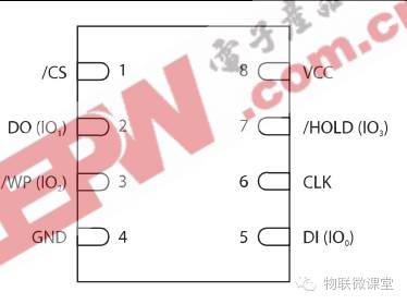
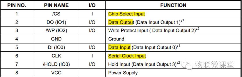 CS chip select signal, DO serial output, DI serial input, CLK serial clock, WP write protection, HOLD hold. Additionally, this chip supports SPI modes 0 and 3, so the host’s SPI can only choose 0 or 3.
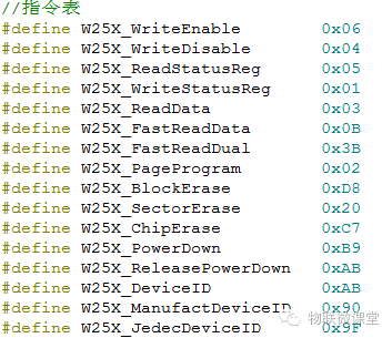
2. Instruction Set
This chip is driven by the SPI bus, so the operation process involves continuously sending data over the SPI bus. Some commands will be sent to the chip, and then the chip will return data.
3. Timing
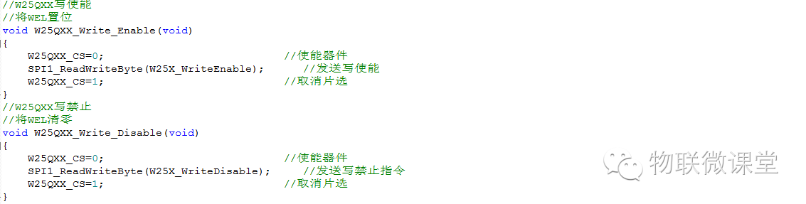
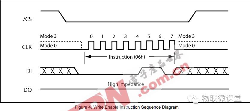
1) Write Enable
Command 06h, pull CS low, and send 06h using the SPI driver.
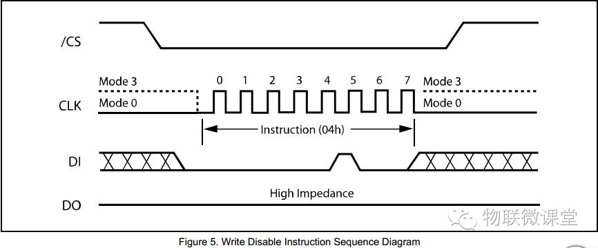
 2) Write Disable
Command 04h, pull CS low, and send 04h using the SPI driver.
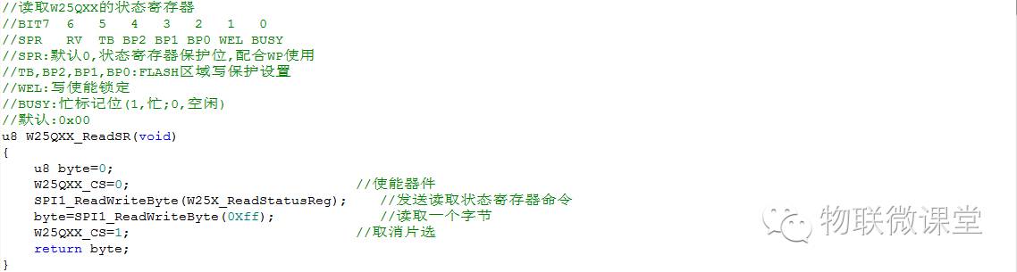
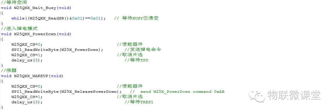
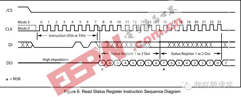
3) Read Status Register
Command 35h, pull CS low, and send 35h using the SPI driver. The status register data will then be returned, and the returned data must be read using the SPI driver.
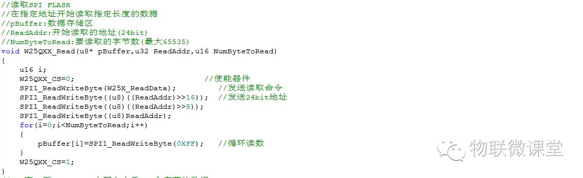
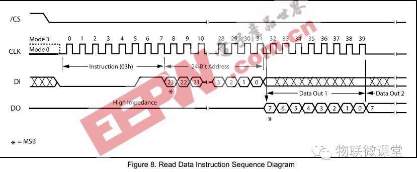
4) Read Data
First send command 03h, then send a 24-bit address (the address must be sent in 3 bytes), and then the data to be read will be returned. Ensure the chip is not in a busy state when reading data.
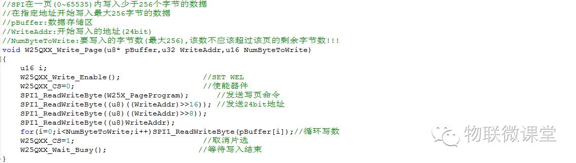
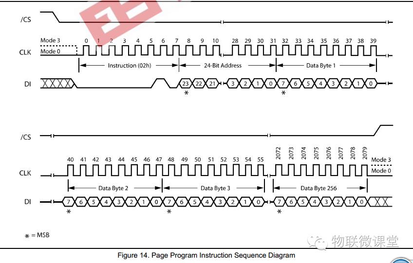
5) Page Programming
Command 02h, then send a 24-bit address, followed by 256 bytes of data to write. Note that the page address must be a multiple of 256.
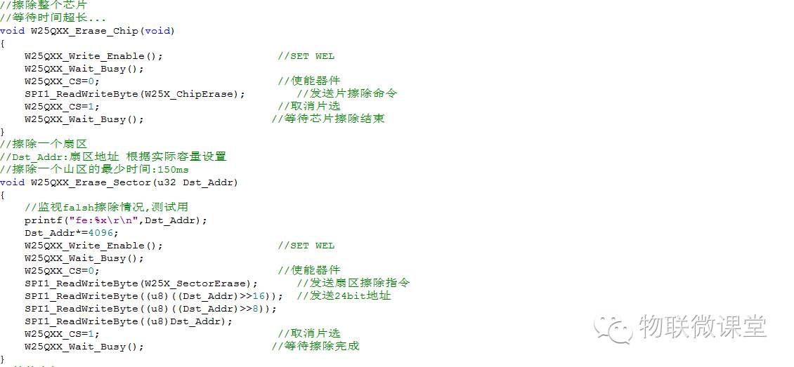
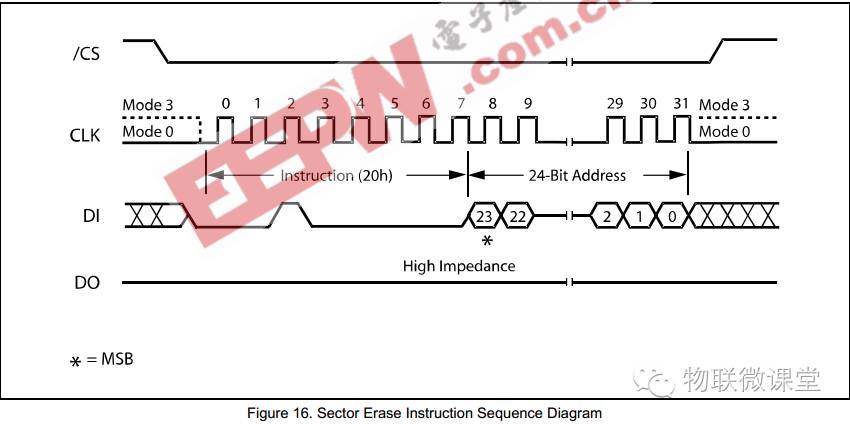
6) Sector Erase
Send command 20h, then send a 24-bit address. The sector address must be a multiple of 4K.
 7) 64K Block Erase
Send command d8h, then send a 24-bit address. The block address must be a multiple of 64K.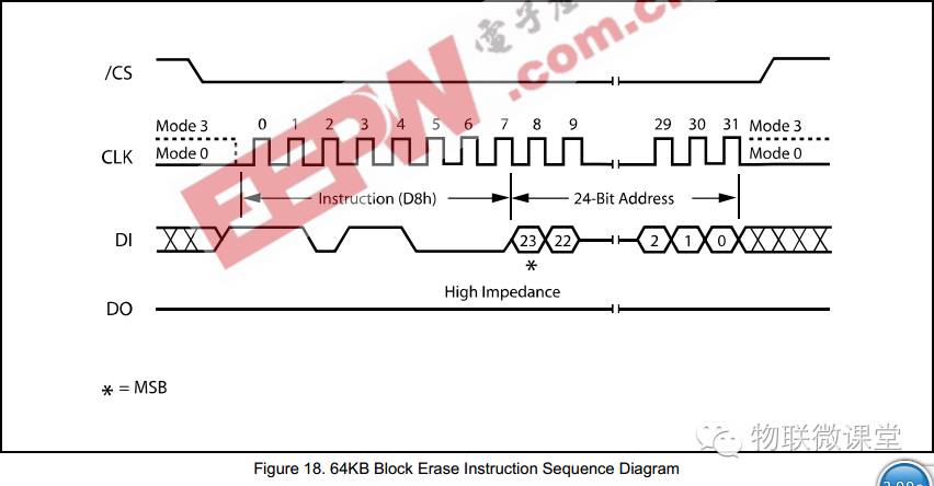 8) Block Erase
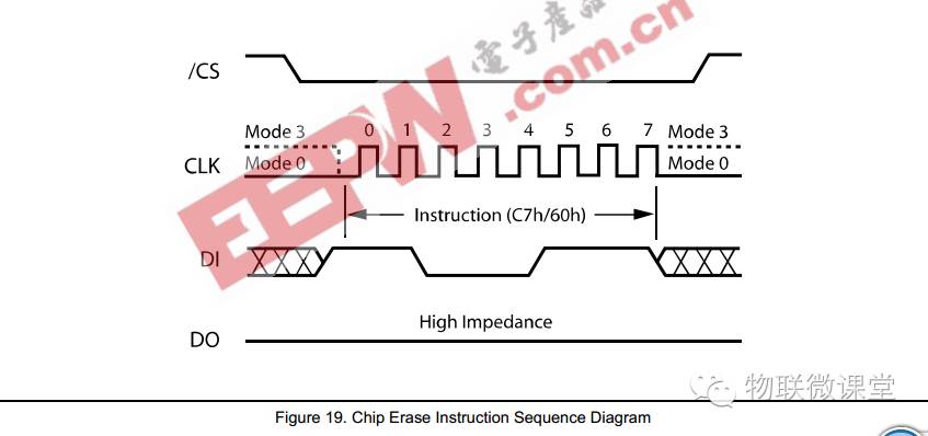
Send command c7h, then send a 24-bit address.
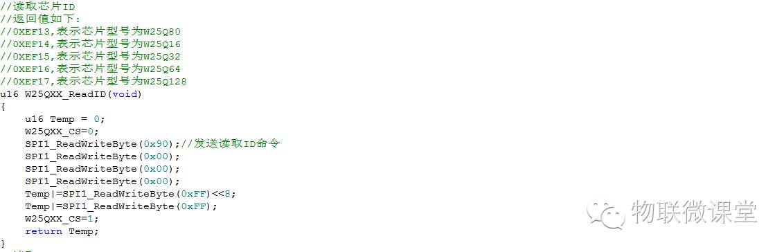
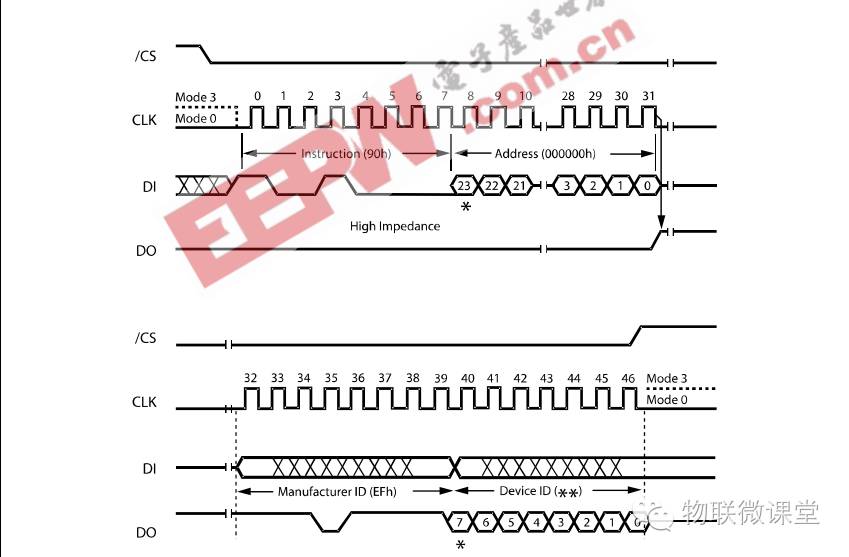
 9) Read Device ID
Send command 90h, then send 3 bytes of 0, and you will receive 2 bytes of ID.
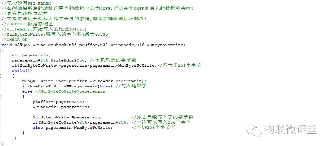
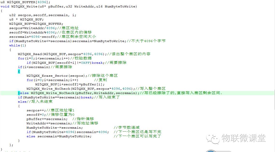
4. Important Notes for Writing Data
1) Since the write operation can only change 1 to 0, it is necessary to erase first.
2) The minimum erase unit is a 4K sector, so part of this 4K is reserved for your data, while the other part contains the original data, which cannot be changed. Therefore, it is important to preserve the original data.
3) After erasing 4K, you need to write two parts of data: one part is the original data, and the other part is the data you want to write.
●Code