What is SPI
SPI stands for Serial Peripheral Interface in English, which, as the name suggests, is a serial peripheral device interface. It was first defined by Motorola in its MC68HCXX series processors.
SPI is a high-speed, full-duplex, synchronous communication bus that only occupies four lines on the chip’s pins, saving pin space and providing convenience for PCB layout. It is mainly used between EEPROM, FLASH, real-time clocks, AD converters, as well as digital signal processors and digital signal decoders.
SPI Master-Slave Mode
SPI is divided into master and slave modes. An SPI communication system requires one (and only one) master device and one or more slave devices. The master device (Master) provides the clock, while the slave device (Slave) receives the clock. The read and write operations of the SPI interface are initiated by the master device. When there are multiple slave devices, they are managed through their respective chip select signals.
SPI is full-duplex and does not define a speed limit. Typical implementations can achieve speeds of 10 Mbps or more.
SPI Signal Lines
The SPI interface generally uses four signal lines for communication:
SDI (Serial Data Input), SDO (Serial Data Output), SCK (Serial Clock), CS (Chip Select)
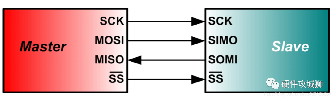
MISO: Master In Slave Out pin. This pin sends data in slave mode and receives data in master mode.
MOSI: Master Out Slave In pin. This pin sends data in master mode and receives data in slave mode.
SCLK: Serial clock signal generated by the master device.
CS/SS: Slave Select signal controlled by the master device. Its function is to act as a ‘chip select pin’, allowing the master device to communicate with a specific slave device, avoiding conflicts on the data lines.
Hardware Consists of 4 Lines.
SPI One-to-One
SPI One-to-Many
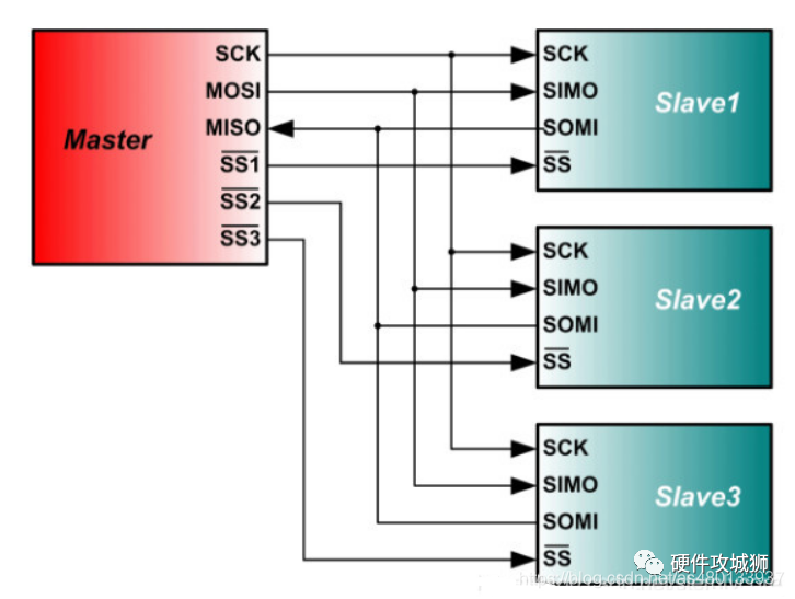
SPI Device Selection
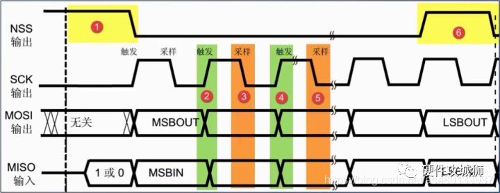
SPI is a single-master communication protocol, which means that only one central device in the bus can initiate communication. When the SPI master device wants to read/write to a slave device, it first pulls down the corresponding SS line (SS is active low), then begins sending clock pulses on the clock line. During the corresponding pulse time, the master device sends signals via MOSI to achieve ‘write’, while it samples MISO to achieve ‘read’, as shown below:
SPI Data Transmission and Reception
Both the SPI master and slave have a serial shift register. The master initiates a transmission by writing a byte to its SPI serial register.
First, pull down the corresponding SS signal line to indicate communication with that device.
The master sends the SCLK clock signal to tell the slave whether to write or read data.
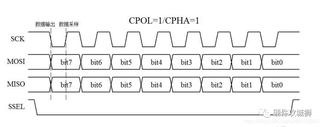
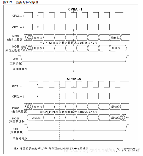
It is important to note that the SCLK clock signal can be active low or active high, as SPI has four modes, which we will introduce below.
The master writes the data to be sent into the transmit data buffer (Memory), and the buffer goes through the shift register (0-7), with the serial shift register sending the byte one bit at a time via the MOSI signal line to the slave, while the data received via the MISO interface moves one bit at a time into the receive buffer.
The slave also returns the contents of its serial shift register (0-7) to the master via the MISO signal line. Simultaneously, it receives the data sent by the master via the MOSI signal line, thus exchanging the contents of both shift registers.
SPI only distinguishes between master and slave modes, without the concept of read and write. The write and read operations of the peripheral are completed synchronously. If only a write operation is performed, the master only needs to ignore the received byte; conversely, if the master wants to read a byte from the slave, it must send an empty byte to trigger the slave’s transmission. In other words, sending a data byte will always result in receiving a data byte; to receive a data byte, the master must first send a data byte.
Four Modes of SPI Communication
SPI has four different operation modes, which simply set the signal on the SCLK clock line as the active signal.
There are 4 different operational modes for SPI communication, and different slave devices may be factory-configured to a certain mode, which cannot be changed; however, both parties in communication must operate in the same mode. Therefore, we can configure the SPI mode of our master device through CPOL (Clock Polarity) and CPHA (Clock Phase) to control the communication mode of our master device, as detailed below:
Clock Polarity (CPOL) defines the idle state level of the clock:
CPOL=0 means that when SCLK=0, it is in idle state, so the active state is when SCLK is high.
CPOL=1 means that when SCLK=1, it is in idle state, so the active state is when SCLK is low.
Clock Phase (CPHA) defines the data sampling time.
CPHA=0 samples data on the first clock edge (rising or falling), and sends data on the second edge.
CPHA=1 samples data on the second clock edge (rising or falling), and sends data on the first edge.
For example:
Mode0: CPOL=0, CPHA=0: At this time, in idle state, SCLK is low, data is sampled on the first edge, which is the transition of SCLK from low to high, so data is sampled on the rising edge (data preparation), and data is sent on the falling edge.
Mode1: CPOL=0, CPHA=1: At this time, in idle state, SCLK is low, data is sent on the first edge, which is the transition of SCLK from low to high, so data is sampled on the falling edge, data is sent on the rising edge.
Mode2: CPOL=1, CPHA=0: At this time, in idle state, SCLK is high, data is sampled on the first edge, which is the transition of SCLK from high to low, so data is sampled on the falling edge, data is sent on the rising edge.
Mode3: CPOL=1, CPHA=1: At this time, in idle state, SCLK is high, data is sent on the first edge, which is the transition of SCLK from high to low, so data is sampled on the rising edge, data is sent on the falling edge.
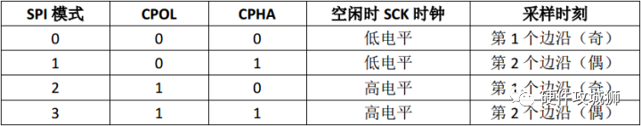
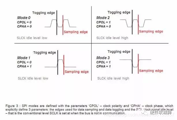
The differences define which edge of the clock pulse toggles the output signal, which edge samples the input signal, and the stable level of the clock pulse (whether the clock signal is high or low when inactive). Each mode is characterized by a pair of parameters known as clock polarity (CPOL) and clock phase (CPHA).
SPI Communication Protocol
The master and slave devices must use the same operating mode—SCLK, CPOL, and CPHA—to work correctly. If there are multiple slave devices, and they use different operating modes, the master device must modify the corresponding slave device’s mode when reading/writing to different slave devices. This is the main content of the SPI bus protocol.
Does it feel like this is the end? That’s SPI. It does not specify a maximum transmission rate, does not have an addressing scheme, does not define a communication acknowledgment mechanism, and does not specify flow control rules.
As long as the four signal lines are connected correctly, the SPI modes are the same, and the CS/SS signal line is pulled low, direct communication can occur, transferring one byte at a time, reading and writing data simultaneously—that’s SPI.
These communication controls must be implemented by the SPI devices themselves, as SPI does not concern itself with the electrical characteristics of the physical interface, such as the standard voltage of the signals.
PS: This is also a disadvantage of the SPI interface: there is no specified flow control and no acknowledgment mechanism to confirm whether data has been received.
Three Modes of SPI
SPI operates in three modes: run, wait, and stop.
Run Mode
This is the basic operational mode.
Wait Mode
When SPI operates in wait mode, it is a configurable low-power mode, controlled by the SPICR2 register’s SPISWAI bit. In wait mode, if the SPISWAI bit is cleared to 0, SPI operations are similar to run mode. If the SPISWAI bit is set to 1, SPI enters a low-power state, and the SPI clock will be turned off. If SPI is configured as a master, all transmissions will stop, but will resume once the CPU enters run mode. If SPI is configured as a slave, it will continue to receive and transmit one byte, ensuring synchronization with the master.
Stop Mode
To reduce power consumption, SPI is inactive in stop mode. If SPI is configured as a master, ongoing transmissions will stop, but will resume once the CPU enters run mode. If SPI is configured as a slave, it will continue to receive and send one byte, ensuring synchronization with the master.
SPI Circuit Connection Diagram
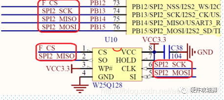
**
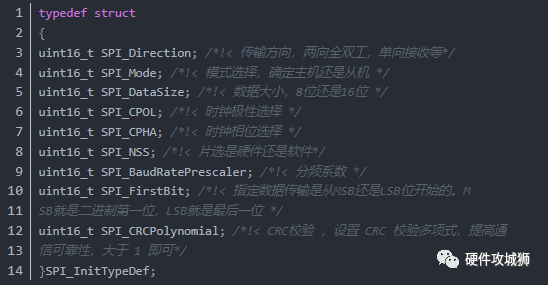
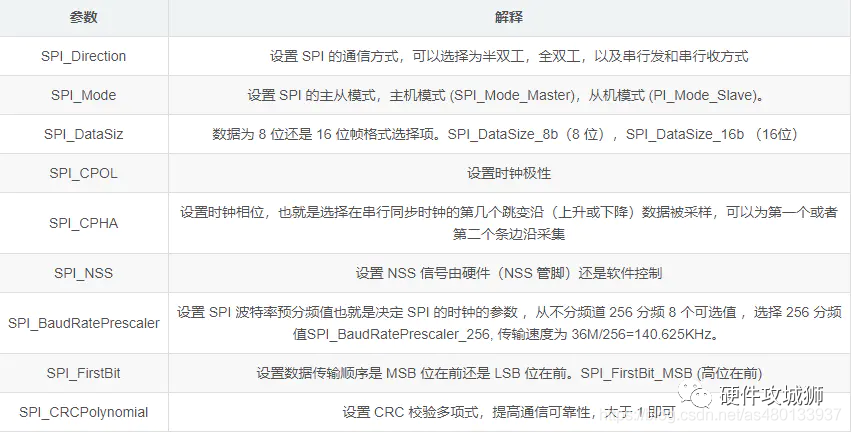
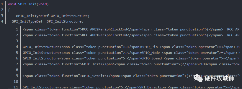
STM32 SPI Initialization Configuration
1. Initialize GPIO ports, configure the multiplexing function of the relevant pins, and enable the SPIx clock. Call function: void GPIO_Init();
2. Enable the SPI clock bus: RCC_APB2PeriphClockCmd(RCC_APB2Periph_SPI1,ENABLE)
3. Configure the parameters for SPI initialization, set the SPI operating mode: SPI_Init(SPI1,&SPI_Initstructure)
4. Enable the SPI peripheral: SPI_Cmd(SPI1,ENABLE);
SPI Configuration Settings
}
SPI Send Function (Standard Library/HAL Library)
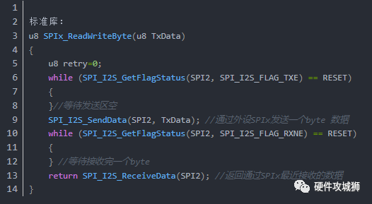
HAL Library:uint8_t SPI_SendByte(uint8_t byte){uint8_t d_read,d_send=byte;if(HAL_SPI_TransmitReceive(&hspi1,&d_send,&d_read,1,0xFFFFFF)!=HAL_OK)d_read=0XFF;return d_read;
Copyright Notice: This article is an original work by CSDN blogger ‘Z Xiaoxuan’, following the CC 4.0 BY-SA copyright agreement. Please attach the original source link and this statement when reprinting.
Original link: https://blog.csdn.net/as480133937/article/details/105764119
 Statement: This article is reprinted from ‘CSDN’, and the copyright belongs to the author. If there is any infringement, please contact us for deletion!
👇 Click Follow, Technology to receive timely delivery of technical content!👇

-
This article clearly explains the DCDC layout, saved after reading
-
The US announces the suspension of EDA supply
-
Understand all knowledge points of WiFi in one article
-
How does a charger not output voltage when not connected to a battery?
-
Jump out of the engineer’s trap
-
Tips for disassembling various components, how many do you know?
-
Eight-layer PCB design, analysis of computer motherboard design
-
After soldering nearly 40 boards, made a high-voltage power supply
-
The tragedy of R&D personnel—’Ponzi scheme’
-
Detailed explanation of power MOSFET (53-page PPT)