Some things can only be done alone. Some doors can only be passed alone. Some roads can only be walked alone.
1. Overview
It is a synchronous serial bus interface specification developed by Motorola in the mid-1980s (with clock signal, controlled by clock polarity and clock phase for sampling, that is, synchronous transmission).
1. Supports half-duplex and full-duplex communication modes.
2. There is no flow control or acknowledgment mechanism to confirm whether data has been received (UART has checks or flow control).
3. There is no fixed transmission rate specification; existing devices have SPI output rates exceeding 50Mbps (I2C has a clear specified rate).
4. Only short-distance transmission on the board (RS232, RS485 output distances are longer).
5. No limit on the number of transmitted bits; commonly used are 8-bit or 9-bit.
6. No hardware address is needed (I2C requires an address), using chip select instead.
7. Master-slave mode, one-to-many.
2. 3-Wire and 4-Wire Modes
Signal definitions for 3-wire SPI and 4-wire SPI in each mode:
3-wire 9-bit Type I interface signals: SCL, CS, SDA
3-wire 9-bit Type II interface signals: SCL, CS, SDO, SDI
4-wire 8-bit Type I interface signals: SCL, CS, DCX, SDA
4-wire 8-bit Type II interface signals: SCL, CS, DCX, SDO, SDI
3-wire 9-bit 2 data lane interface signals: SCL, CS, D0, D1
Distinguishing between 3-wire and 4-wire is not about the number of signal lines, nor is it about half-duplex and full-duplex, or differences in the number of data lines.
Personally, I believe:
3-wire refers to clock, chip select, and data signal (regardless of whether there is one or two data lines), a total of three types of signals.
4-wire refers to clock, chip select, data signal, and data or command control line (determining whether data or command is sent), a total of four types of signals.
3. Four Operating Modes of SPI
The four operating modes are obtained through the combination of CPOL clock polarity and CPHA clock phase:
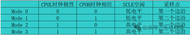
CPOL clock polarity defines the level of the SCLK clock line when idle.
CPOL=0, that is, SCLK=0, indicates that the SCLK clock signal line is at a low level when idle, thus the effective state is high.
CPOL=1, that is, SCLK=1, indicates that the SCLK clock signal line is at a high level when idle, thus the effective state is low.
CPHA clock phase defines the timing (i.e., phase) of the data bits relative to the clock line.
CPHA=0 indicates that the output (out) side changes data at the falling edge of the previous clock cycle, while the input (in) side captures data at the rising edge of the clock cycle (or shortly thereafter).
The output side holds the data valid until the end edge of the current clock cycle. For the first clock cycle, the first bit of data must appear on the MOSI line before the clock rising edge. Thus, a CPHA=0 cycle includes half a clock idle and half a clock set period.
CPHA=1 indicates that the output (out) side changes data at the rising edge of the current clock cycle, while the input (in) side captures data at the falling edge of the clock cycle (or shortly thereafter).
The output side holds the data valid until the rising edge of the next clock cycle. For the last clock cycle, the slave device keeps the MISO signal line valid until the chip select signal disappears. Thus, a CHPA=1 cycle includes half a clock set and half a clock idle period.
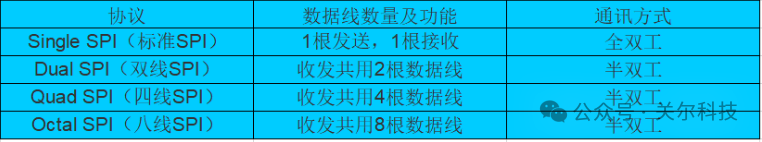
4. Upgraded Version of SPI
The SPI flash interface has standard SPI, Dual SPI, Quad SPI, and Octal SPI, which correspond to 1, 2, 4, and 8 wire modes.
5. SDR and DDR Modes
SPI communication supports SDR and DDR modes.
SDR: Single Data Rate samples the signal triggered by SCLK once per clock cycle, referred to as single data rate mode.
DDR: Double Data Rate samples the signal triggered by SCLK once on each rising and falling edge.
That is, sending or receiving 2 bits of data within one clock cycle is referred to as double data rate mode.
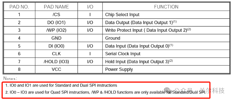
6. SPI Flash Interface
Dual SPI has two data IO; Quad SPI has four data IO.
SPI flash spec:
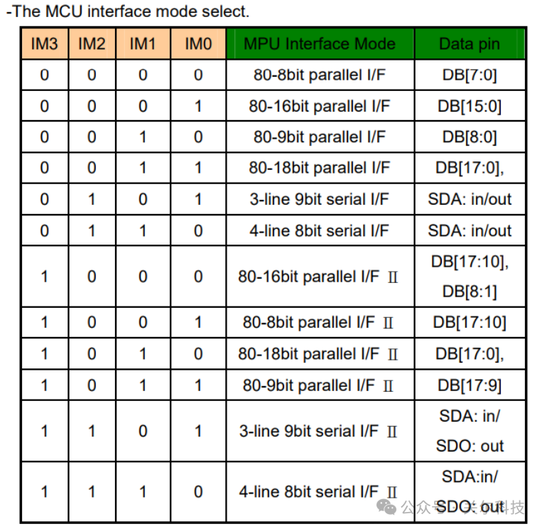
7. SPI TFT LCD Screen Interface
The TFT LCD screen ST7789 spec defines support for serial and parallel communication, supporting various SPI communication modes.
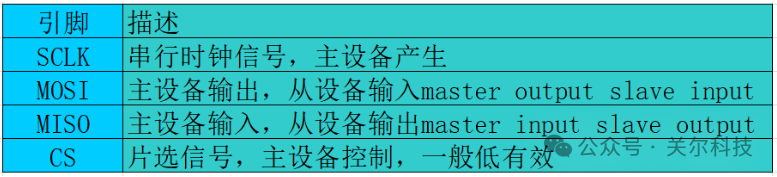
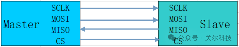
8. Signal Definitions and Wiring
Standard SPI interface signal definitions:
Standard SPI specification wiring:
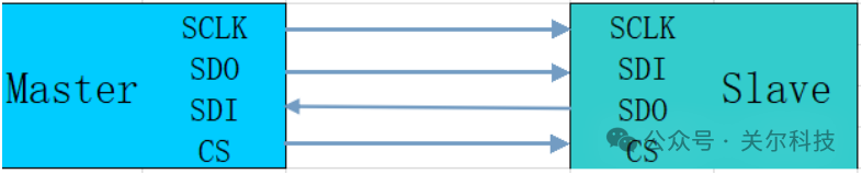
SDO/SDI network naming wiring (SDO and SDI crossed):
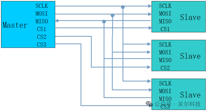
SPI bus, one-to-many wiring:
9. Summary
1. In some reference design schematics, SDI is used to indicate MOSI, and SDO is used to indicate MISO; pay attention to the definitions of output and input in wiring.
2. The signal input or output of chip pins is marked for itself, so the output or input of master-slave devices must be connected correctly.
3. In circuit design, pin signals do not need pull-ups. If it is IO simulation, be aware of whether it is open-drain; if so, a pull-up should be added. Additionally, confirm the device spec’s SPI information, as there may be special pull-down requirements.
4. For one-to-many wiring, the chip select signal CS is controlled separately, requiring multiple CS signals for multiple slave devices.
5. When the slave device is not selected, the signal line becomes high impedance (disconnected).
6. There are no special requirements for layout; of course, the SCLK signal can be grounded.
END
———————————————-
The jungle society never believes in tears; no amount of complaints will help; no one will pity you;
Long press to follow
More attitude
Guang’er Hardware