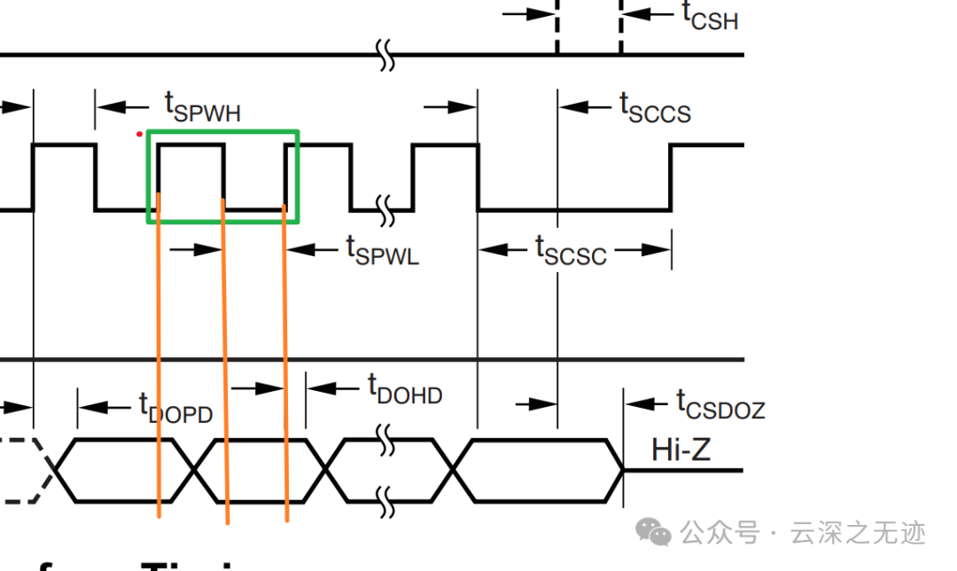
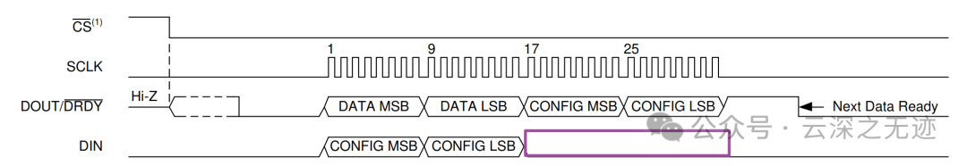
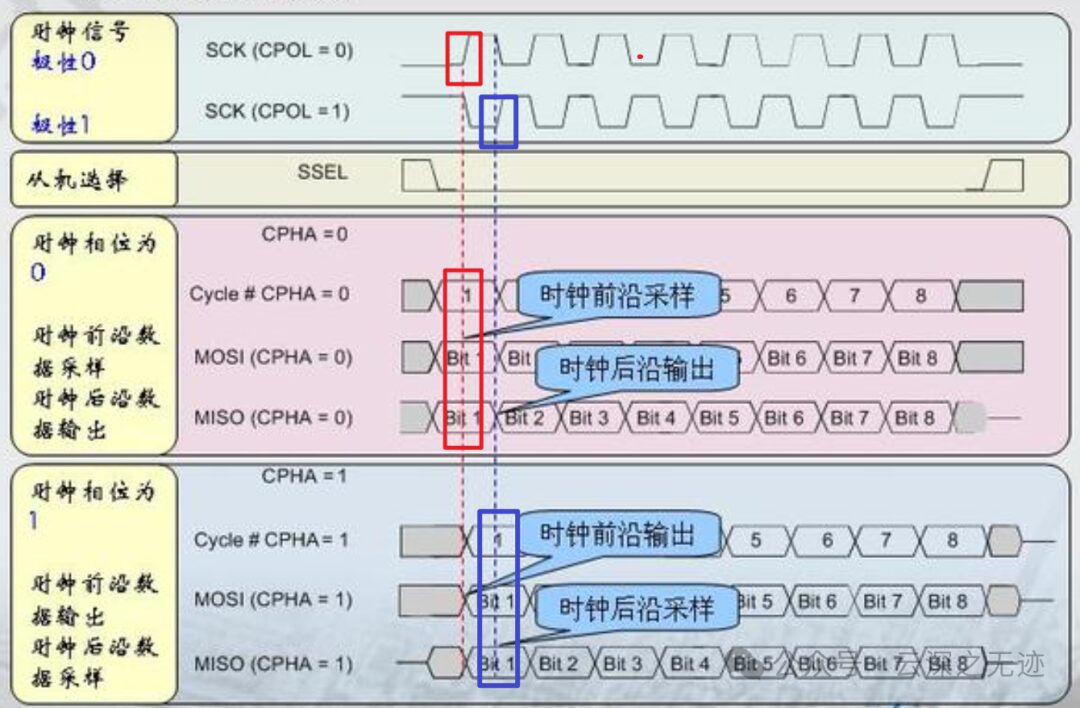
This is the timing diagram. Because it is bidirectional transmission, during the time the master sends to the slave, the slave is also sending data, but it is essentially sending meaningless data:
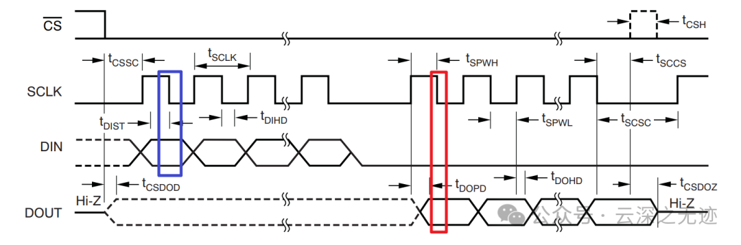
Additionally: The sealed rhombus part should be noted to be sealed, indicating valid data, and the term Valid Data also reflects this.
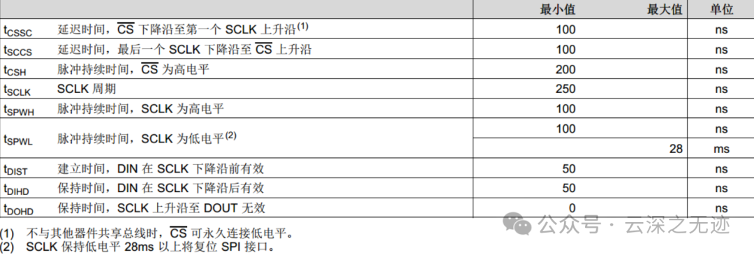
Regarding the time annotations, this is also very important information, as these time annotations indicate the minimum or maximum time that certain states must be maintained.
Because the operating speed of the device is also limited, it generally cannot keep up with the speed of the master control chip, so there must be timing coordination between them.
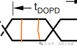
The external 12MHz crystal oscillator means that the instruction cycle is one clock cycle, which is (1/12MHz) us, so it at least confirms that the time to execute one instruction is at the us level. We see that all the time parameters given above are at the ns level, so even if we do not add delay in the program
10 to the power of -3
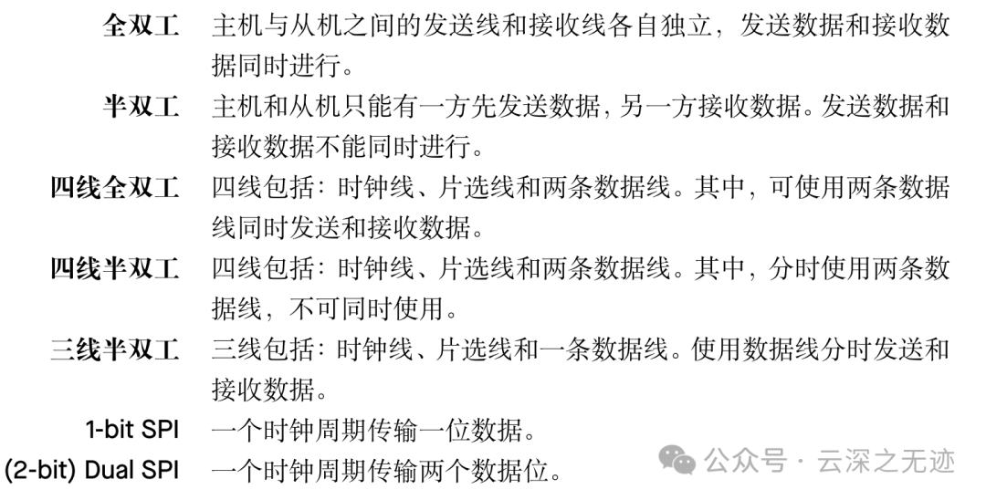
Timing
The dedicated clock pin has Schmitt input.
This name is good, DIN, and the data latch exists on the falling edge:

GPIO has enabled the weak pull-up resistor on the pin:
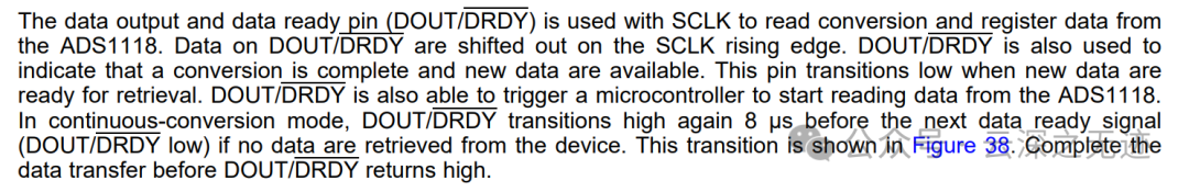
The rising edge is moving out, and the falling edge is preparing:
This is one clock cycle of output
The meaning of this is that the data has highs and lows, the later line is data output, and the front is data preparation. Or it is latched
Not sure if all are like this. Similar to the above analysis
Look at a continuous output
On the timing
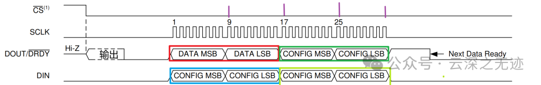
In the data given to the MCU, a large clock cycle consists of 32 small cycles, with two bytes indicating the conversion result, which is the data itself, with MSB first. The last two are the register readback, which I understand as sending the output control command back once.
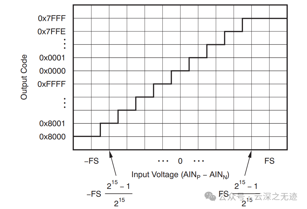
2^16, two 16 bits
DIN is the information given by the MCU to the device. MSB + LSB is sent once, and if the remaining half does not change, you can keep the DIN pin low or high in the next cycle.
You see, it’s like this
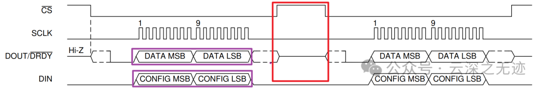
There is also a 16-bit output mode, which can alternately pull CS low to output
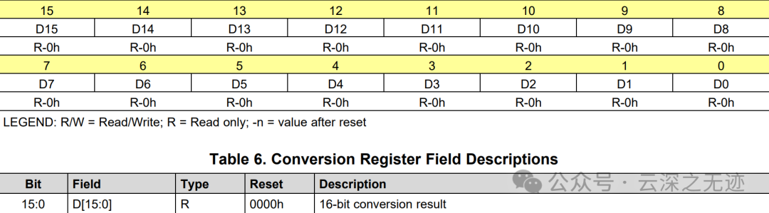
This is what the register for outputting 16-bit values looks like, from 0 to 15, each bit above is either a 0 or 1, a total of 16 bits.
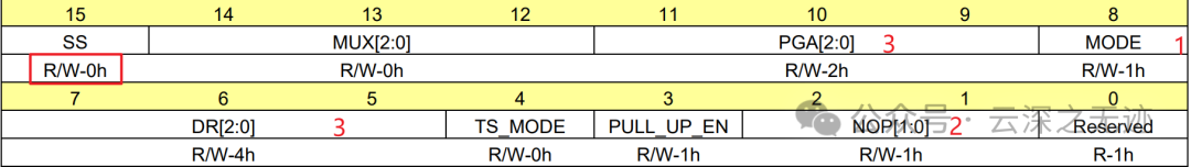
This is the configuration register, starting from 0 and writing up to 15, forming a 16-bit sequence to send.
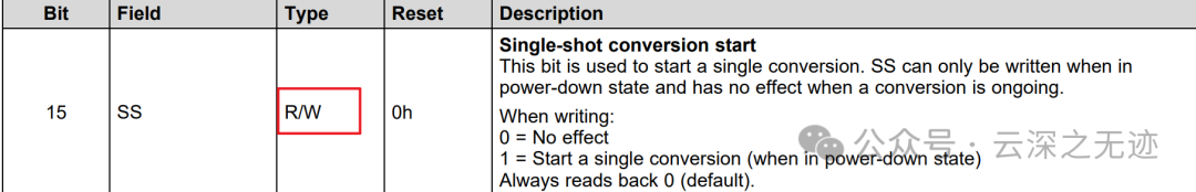
The writing method in the data manual is reversed, starting from 15, stating that this register’s position is at 15, named SS, it can be read and written, and is set to 0h after a restart, indicating it can only be set once during power-off.
This is 3 bits, 8 situations, corresponding to each collection method:
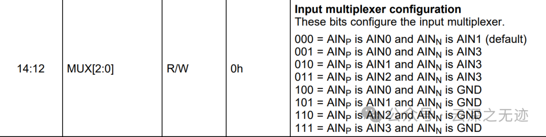
If it’s against ground, then it’s differential
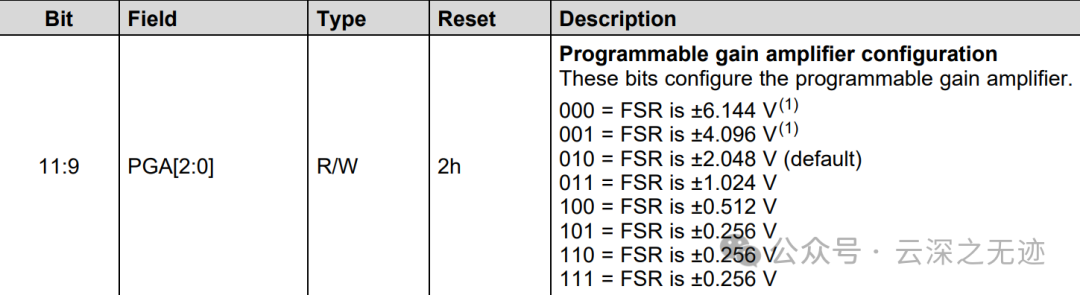
Amplifier:
Rate:
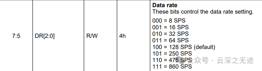
Continuous or single transmission:
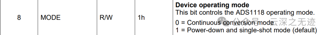
The default is single transmission
I found this image appears the most.
OK
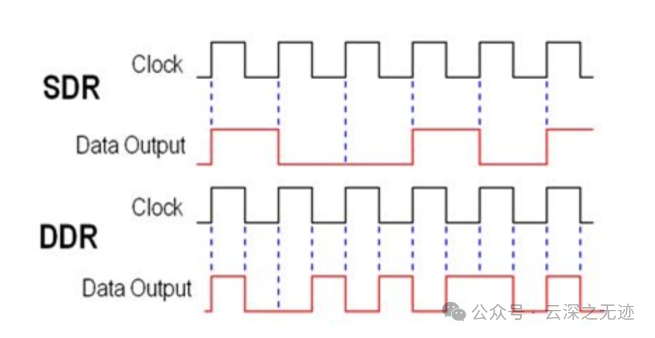
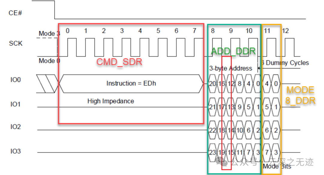
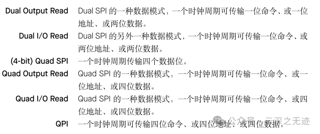
Extended SPI also adds two modes: SDR (Single Data Rate) and DDR (Double Data Rate). In the standard SPI protocol’s SDR mode, data is transmitted only on one edge of SCK, meaning one SCK clock transmits one bit of data; while in DDR mode, data is transmitted on both the rising and falling edges of SCK, meaning one SCK clock can transmit two bits of data, effectively doubling the transmission rate.
That’s how it is
No problem, you can see that the levels on the data line are indeed stable at the internal CLK rising and falling edges, and can be read.
-
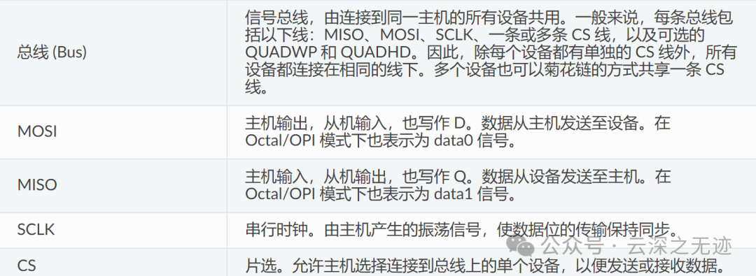
Data lines: Use MOSI and MISO to transmit data simultaneously. -
Data rate: The data transmission rate doubles compared to standard SPI, as it uses two lines to transmit data simultaneously. -
Usage scenario: Suitable for scenarios requiring higher data transmission rates than standard SPI but not needing four-line Quad SPI.
-
Data lines: Usually uses one or more data lines, but transmits data twice for each clock cycle. -
Data rate: The data rate is double that of standard SPI, as it transmits data on both the rising and falling edges of the clock. -
Usage scenario: Suitable for high-performance applications, such as high-speed data acquisition or high-resolution video transmission.

What is HI-Z?
Supplement:
Hi-Z is a common term in digital circuits, referring to a state of output where it is neither high nor low. If the high-impedance state is input to the next circuit, it will have no effect on the downstream circuit, similar to not being connected. If measured with a multimeter, it may show high or low, depending on what is connected to it. High impedance state: In essence, the high impedance state can be understood as an open circuit during circuit analysis.
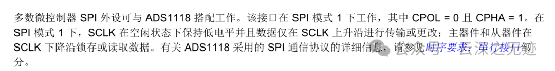
Mode 1:
The rising edge changes, the falling edge reads.
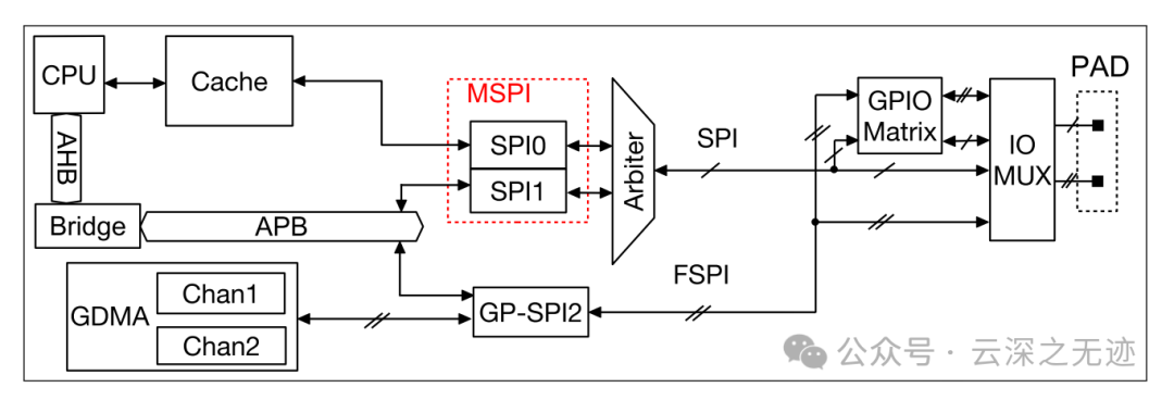
I also have an ESP32-C3 microcontroller at hand, and this is its data manual, which has three SPIs, or one SPI with six CS lines.
External pads, through MUX, multiplexed to the interface, can go through DMA or Cache to the CPU, etc., more on that later.
This is even more professional
The SPI master driver allows multiple devices to be connected on the bus (sharing a single ESP32-C3 SPI peripheral). The driver is thread-safe when each device is accessed by only one task. Conversely, if multiple tasks try to access the same SPI device, the driver is not thread-safe.
All SPI protocols can be divided into these steps.
When the data transfer transaction is equal to or less than 32 bits, allocating a buffer for the data will be the suboptimal choice.
-
Transmission transaction interval time -
SPI clock frequency -
Cache-missing SPI functions, including callbacks
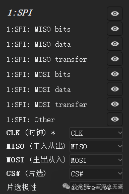
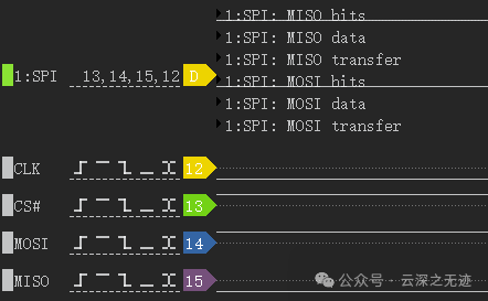
Detailed settings can be made for SPI during capture
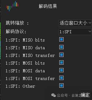
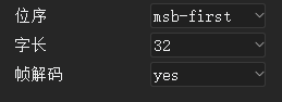
Settings for three decoding levels
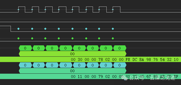
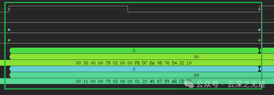
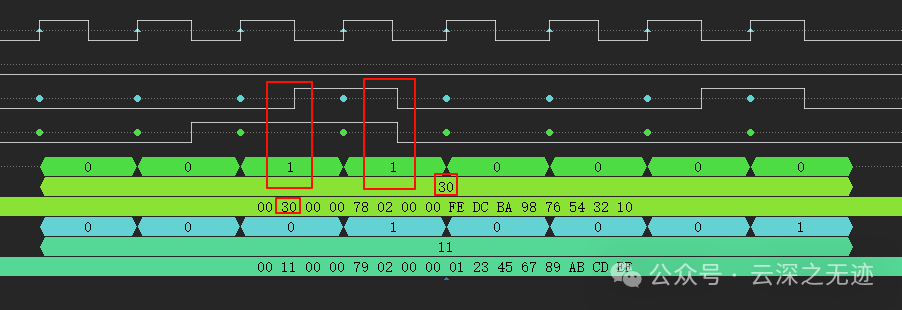
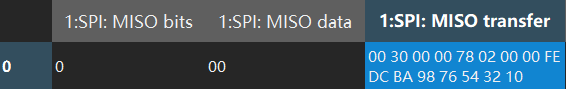
Here, the decoding has several levels, first at the bit level, which is 0, 1, then the conversion, which is 0, 1 combined into other base data. Finally, converting into data.

All zeros
I like using hexadecimal

You can see it is a continuous grouping and assembling process
First, look at the change of the clock
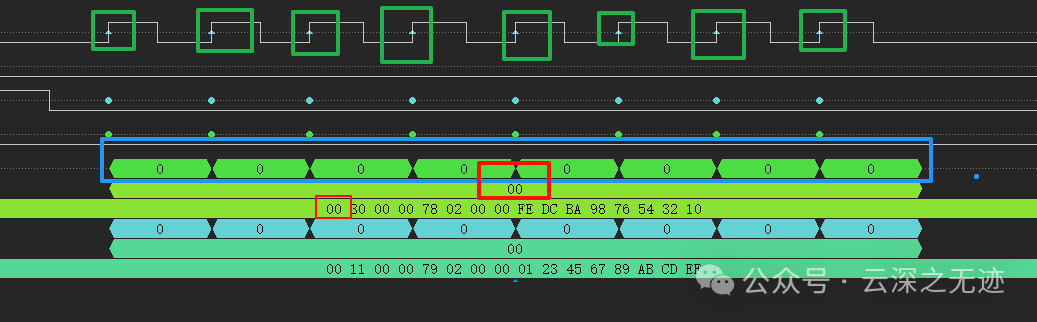
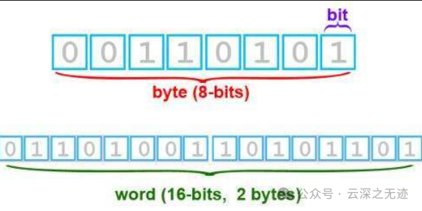
There are eight rising edges, which means 8 zeros, which is the level of conversion, 8 bytes make up one word – 00.
Below are two bytes turned into a word – 16 bits
The second byte

This is roughly the decoding process
This is the first piece of data decoded
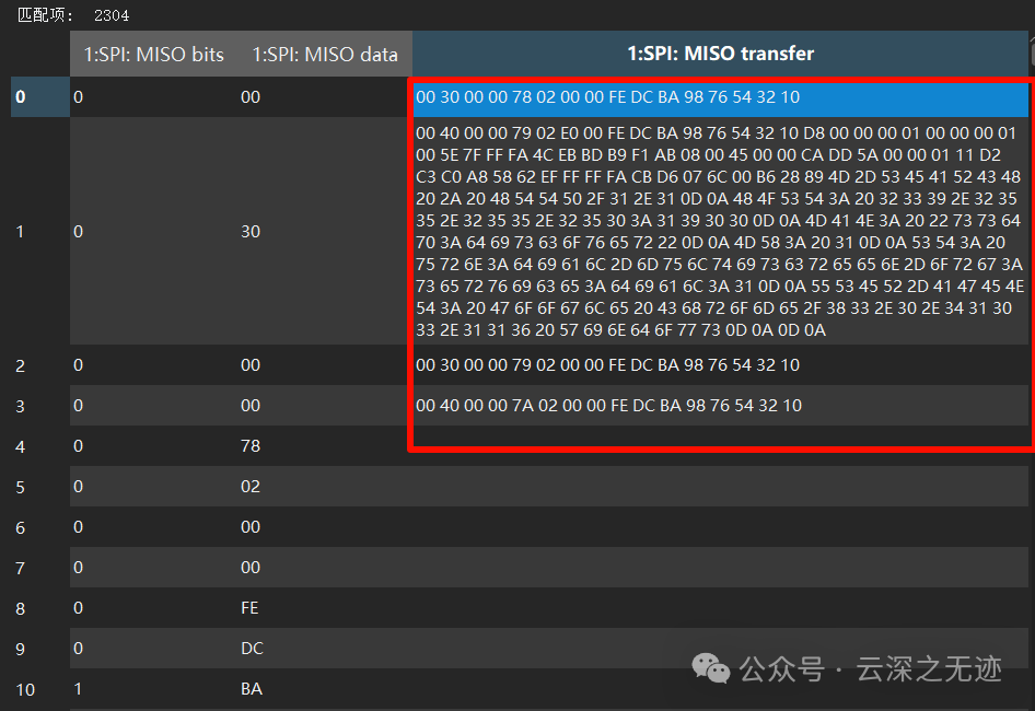
The front is the bit level, the next is the byte level, and the next is the word level
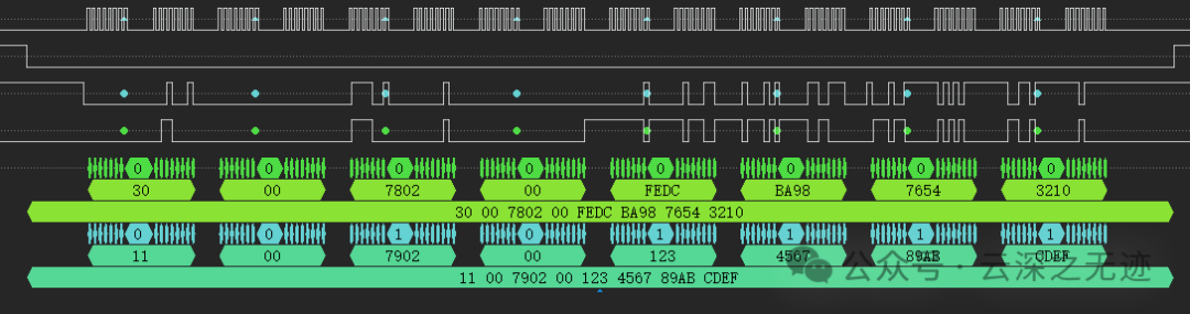
Decode according to 16 bytes
Because it can freely transmit any byte data, you can also define this matter here
Here, it begins to port, looking at the TI’s intention to implement SPI interfaces at will: 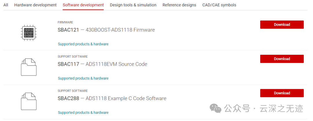
Download the last one
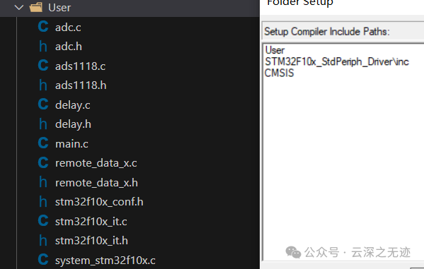
First, let’s talk about how to add header files
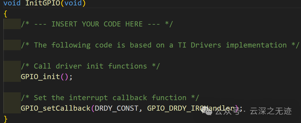
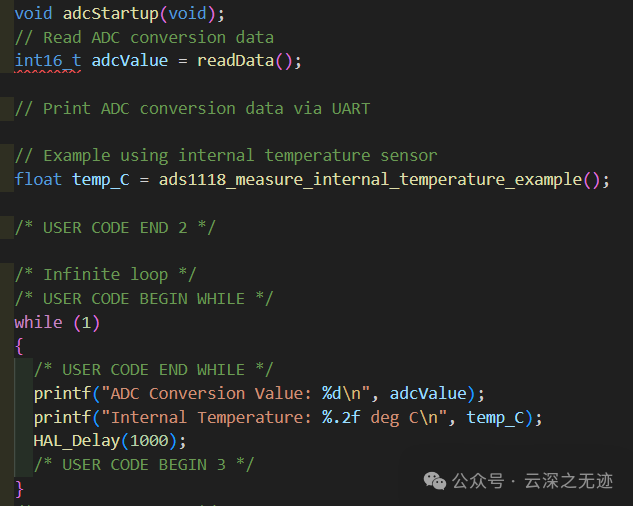
Our task is to implement the STM32 SPI interface porting in the code, and then measure all parameters online to learn SPI in more detail.
First, understand the provided code and clarify what needs to be done:
These are TI’s libraries

This way
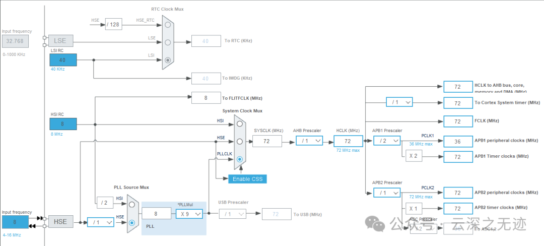
The external crystal oscillator is 8MHz
-
1Select external clock HSE 8MHz
-
2PLL phase-locked loop multiplication by 9 times
-
3System clock source selection is PLL
-
4Set APB1 prescaler to /2
-
5 Enable CSS monitor clock
Later, I found the Chinese data manual
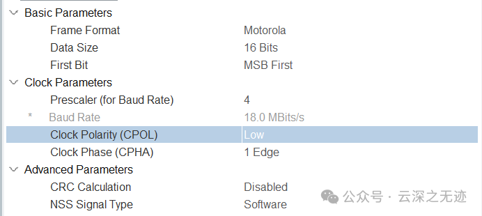
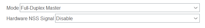
This place has 4 mode selections
Open the window
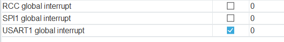
Open the interrupt
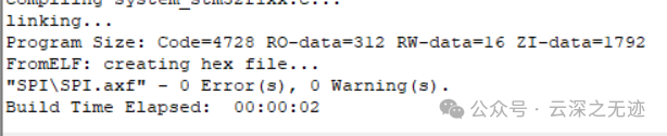
Compile Ok
This is everything from TI’s hardware layer, which will be rewritten soon
I have used TI boards less
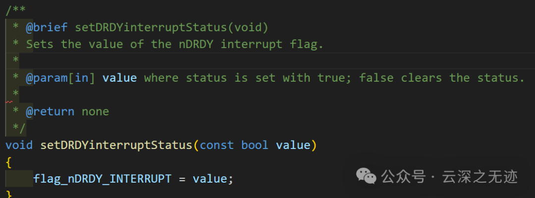
Interrupt status
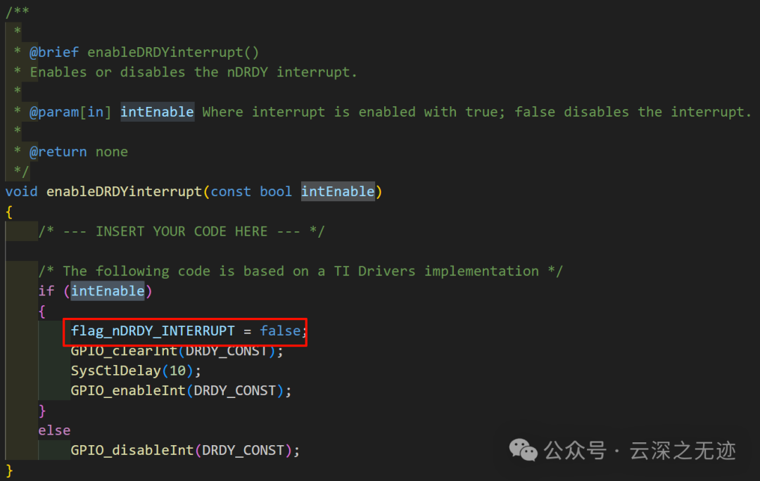
Enable interrupt
Enable interrupt pin
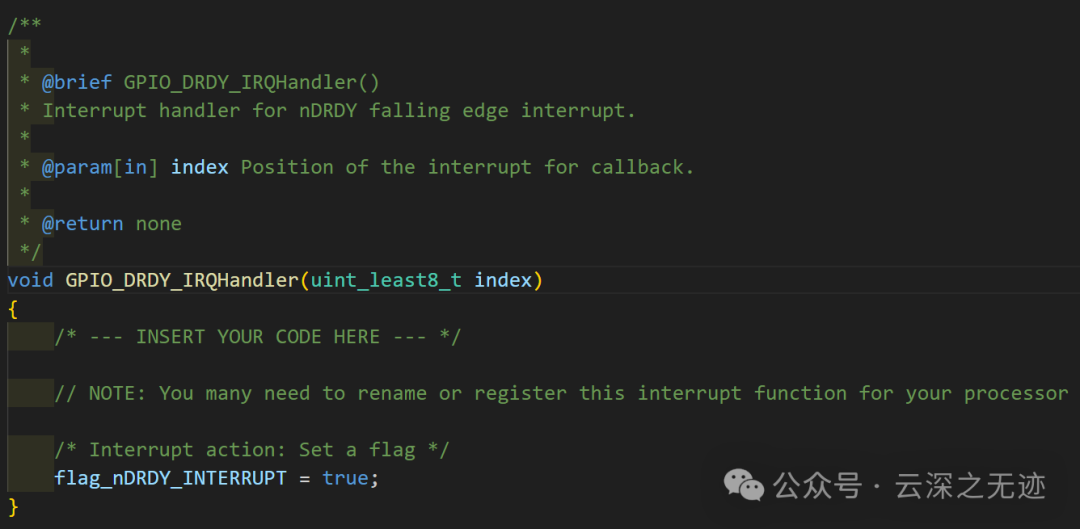
Falling edge triggers interrupt
This is useful
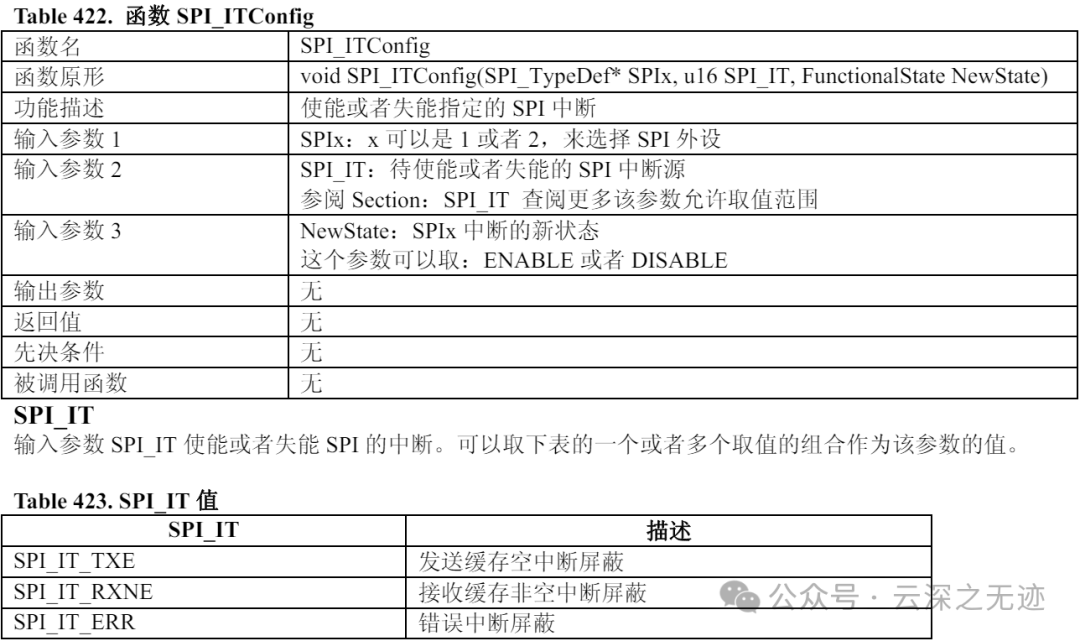
Because the SPI interrupts of STM32 and TI do not match, let’s look at the HAL API:
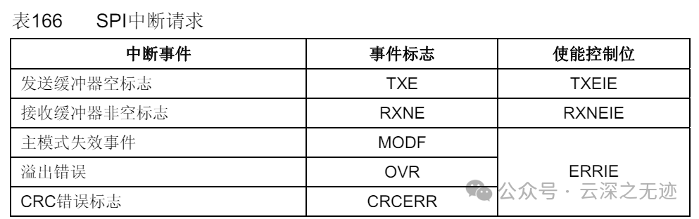
These are the SPI interrupts
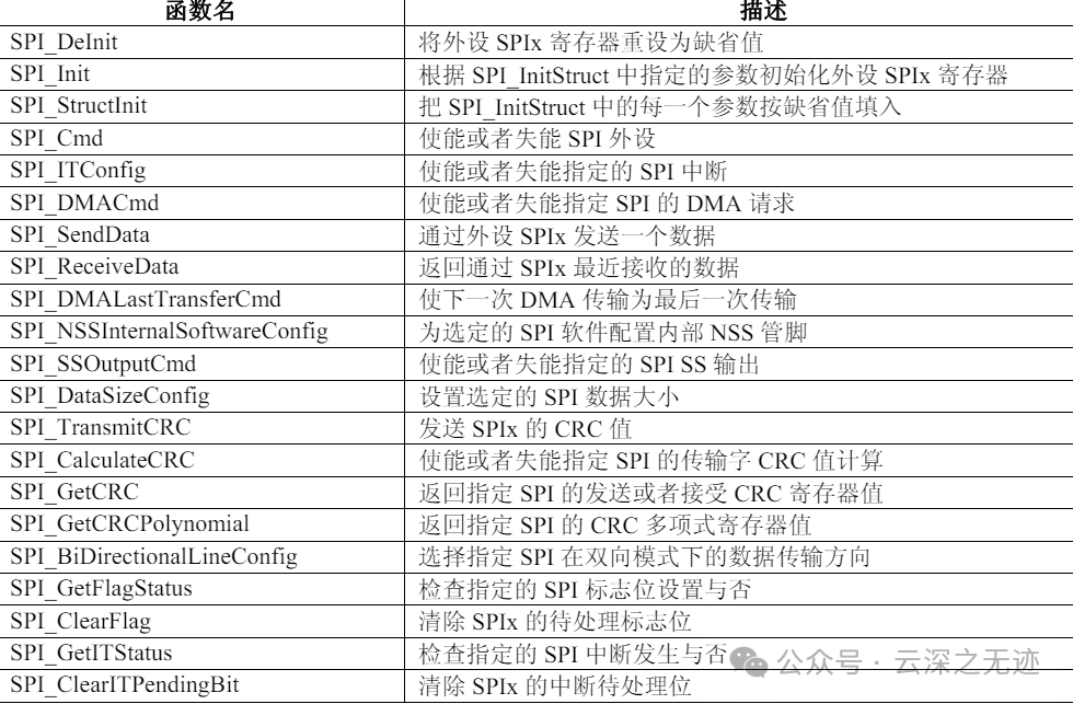
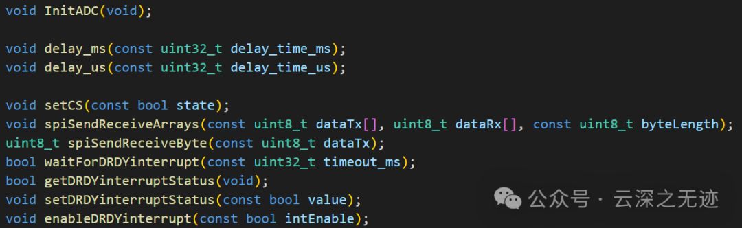
All functions
Interrupt

In the main file inside
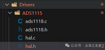
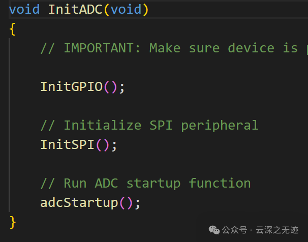
What I need to do is to build the hardware reconstruction of STM32 SPI in the HAL files
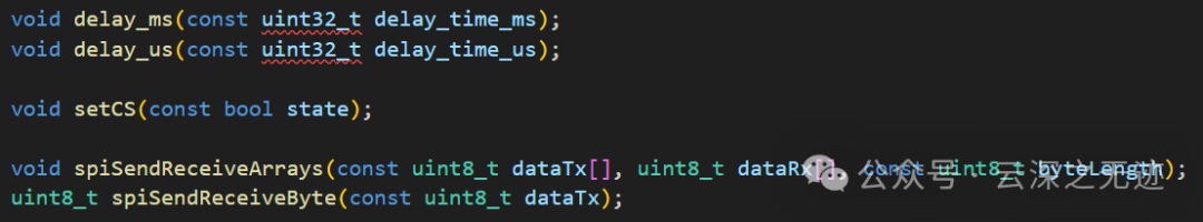
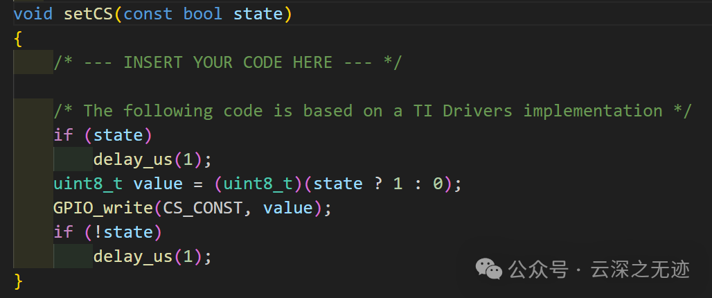
What needs to be implemented is the delay in ms and us, CS control, and transmission and reception functions
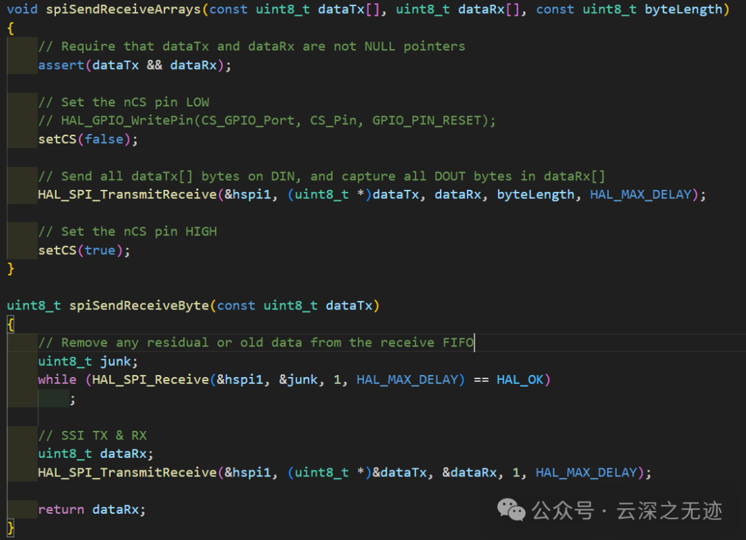
SPI functions
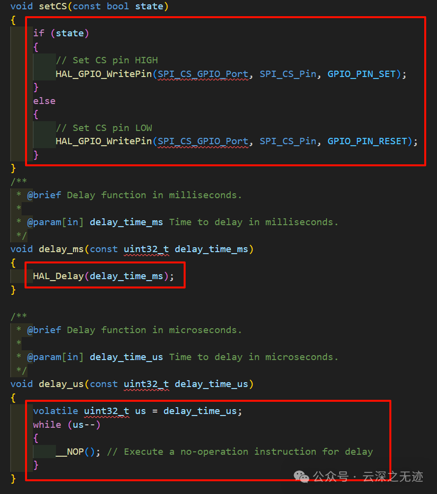
Here is the implementation of delay and CS
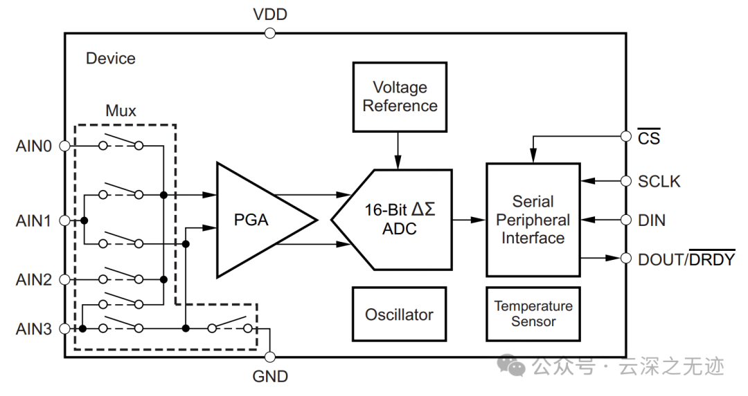
The internal of ADS1118 can be ignored. Don’t be fooled by its simplicity, debugging can also be time-consuming.
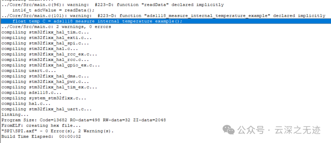
Compiling with no errors, porting completed
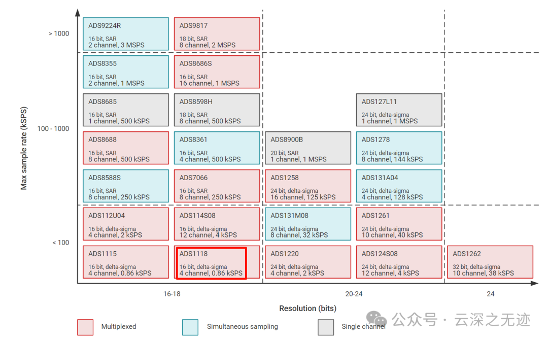
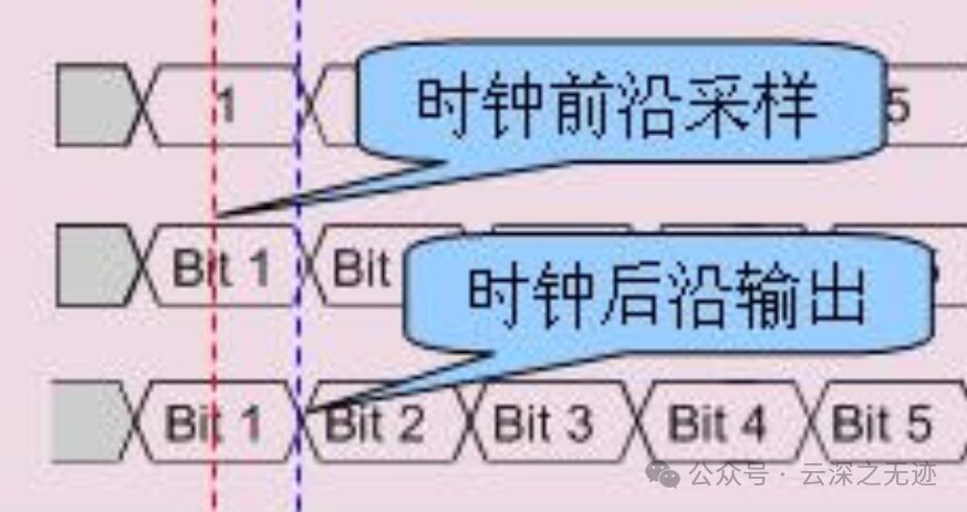
You can take a look at the positioning of ADS1118
https://www.stmcu.com.cn/Designresource/detail/software/711298Glossary:
https://blog.csdn.net/woshiyuzhoushizhe/article/details/90447327https://zhuanlan.zhihu.com/p/146053309https://blog.csdn.net/yangguoyu8023/article/details/111474775https://www.ti.com/product/ADS1118#reference-designs