●SPI Bus
1. What is SPI
SPI is the abbreviation for Serial Peripheral Interface, which is a serial peripheral interface. SPI is a high-speed, full-duplex, synchronous communication bus that occupies only four pins on the chip, saving pin space and providing convenience for PCB layout. Due to its simplicity and ease of use, more and more chips now integrate this communication protocol.
SPI is a ring bus structure consisting of ss(cs), sck, sdi, and sdo. Its timing is quite simple, mainly under the control of sck, where two bidirectional shift registers exchange data. Data is sent on the rising edge and received on the falling edge, with the high bit sent first. When the rising edge arrives, the level on sdo will be sent to the slave device’s register. When the falling edge arrives, the level on sdi will be received into the master device’s register.
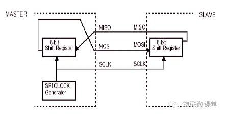
2. SPI Model
 (1)MOSI: Master device data output, slave device data input (2)MISO: Master device data input, slave device data output (3)SCLK : Clock signal generated by the master device (4)/SS: Slave device enable signal controlled by the master device
3. SPI Timing
The SPI interface has four different data transmission timings, depending on the combination of CPOL and CPHL. The following figure displays these four timings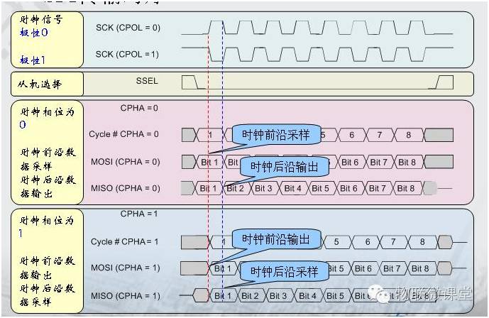
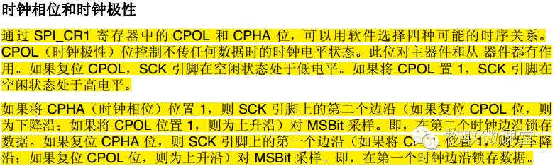
CPOL is used to determine the idle level of the SCK clock signal; CPOL = 0, idle level is low; CPOL = 1, idle level is high. CPHA determines the sampling moment; CPHA=0, samples on the first clock edge of each cycle; CPHA = 1, samples on the second clock edge of each cycle.
The SPI master module and the peripheral communicating with it must have matching clock phase and polarity.
●STM32 SPI Interface
1. Interface Features
1) Full-duplex synchronous transmission based on three lines
2) 8-bit or 16-bit data frames
3) Master mode or slave mode
4) LSB or MSB first
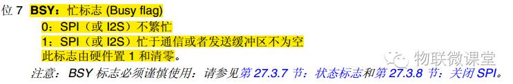
5) SPI bus busy flag
2. Function Description
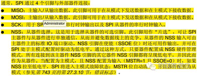
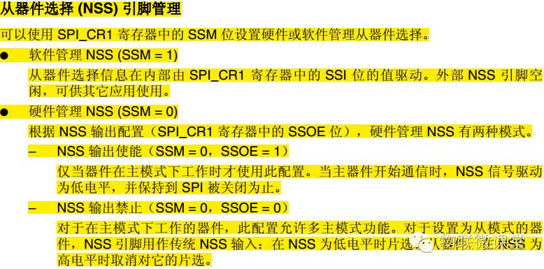
 The NSS pin can be managed by software, which makes it easier to operate. The slave device’s NSS pin can be driven by a GPIO pin of the microcontroller; simply pulling the IO level low can select the slave device.
3. Timing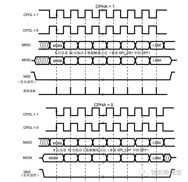 Note that the master device’s phase and polarity must match those of the slave device.
4. Configuring STM32 as Master Device
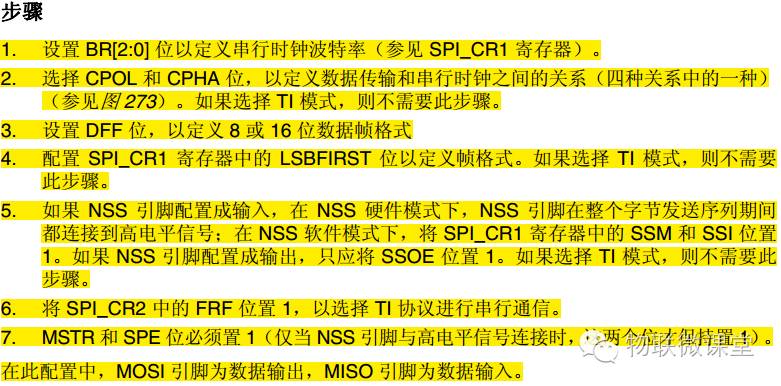
5. Registers
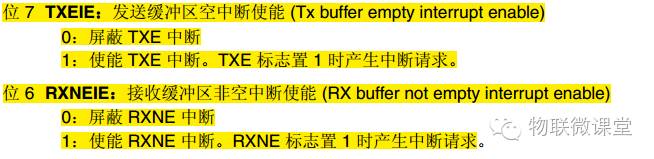
1) Control Register SPI_CR1
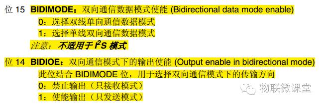
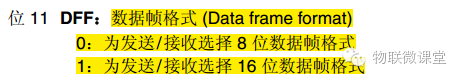
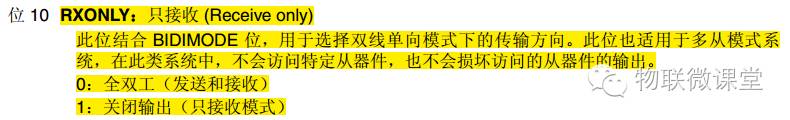
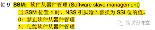
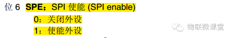
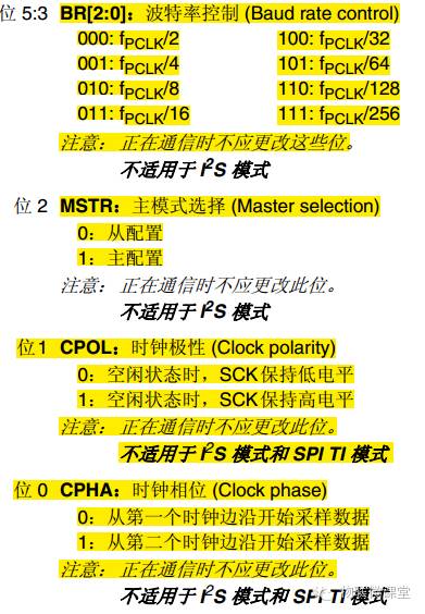
2) Control Register SPI_CR1
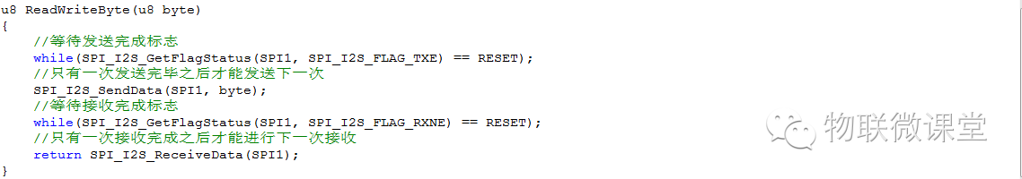
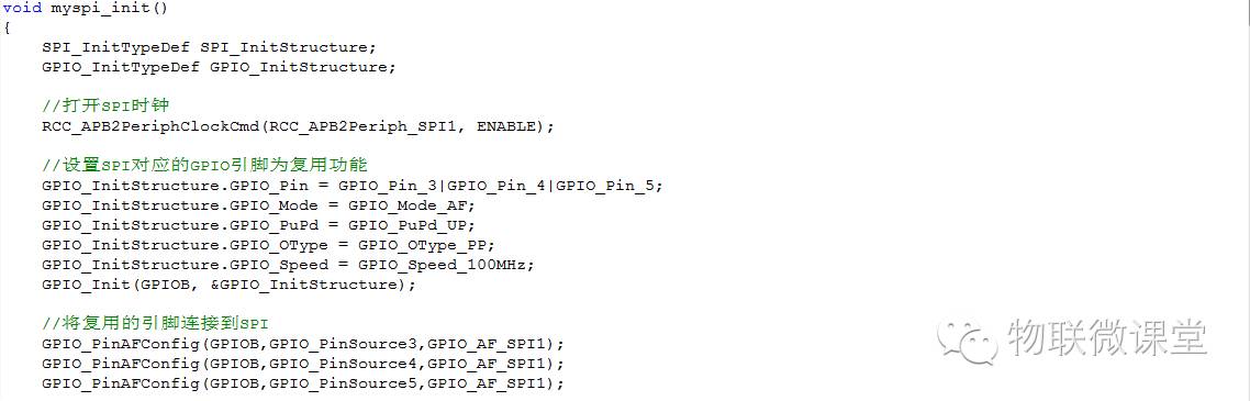
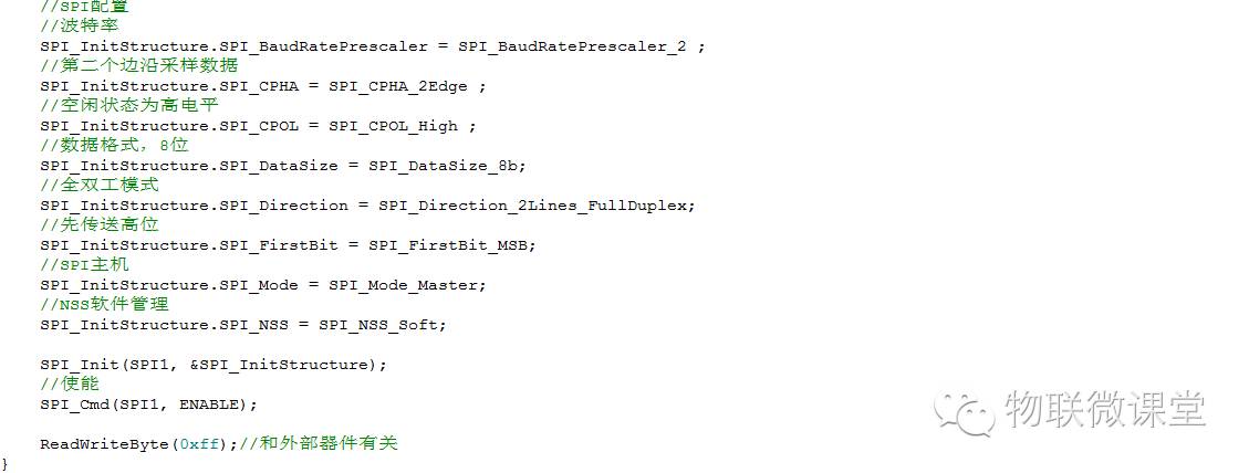
● Code
1. Initialization
2. Data Transmission