Image sensors, as the core gateway of the optoelectronic information era, have profoundly influenced the way humans perceive the world through their technological evolution. From the popularization of digital photography to industrial applications in machine vision, from environmental perception in autonomous driving to precise diagnostics in medical endoscopy, image sensors have become a key hub connecting the physical world with digital intelligence, demonstrating universal value in consumer electronics, industrial inspection, intelligent transportation, and biomedical fields.
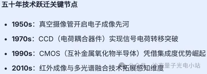
This grand history of technological evolution not only reflects the continuous breakthroughs in semiconductor processes but also mirrors humanity’s relentless pursuit of higher definition, smarter, and broader scene visual perception. From laboratory prototypes to a market scale of tens of billions, the development of image sensors validates the revolutionary role of core device technology in driving the information industry.
Underlying Logic of Optoelectronic Imaging
The essence of optoelectronic imaging is to achieve the precise conversion of optical signals to digital information, which can be analyzed through three dimensions: a three-level conversion mechanism, a chain of core indicators, and constraints of standard specifications.
Three-Level Conversion Mechanism: Light-Electricity-Digital
The imaging process begins with photon absorption, where the photodiode in the photosensitive element converts incident photons into electrons; this is followed by the charge integration phase, where the accumulated electrons form a charge packet proportional to the light intensity; finally, through the quantization readout stage, the analog charge signal is converted into digital encoding by an analog-to-digital converter (ADC), completing the transformation from physical light signals to digital images. This process constitutes the fundamental working principle of all image sensors, determining the core performance boundaries of the imaging system.
Logical Correlation of Core Indicator Chain
The imaging quality is determined by a series of interrelated parameters, forming the quantum efficiency (QE) → full well capacity → dark current → readout noise → dynamic range indicator chain. Quantum efficiency characterizes the ability of the photosensitive element to capture photons, directly affecting the sensor’s light sensitivity; full well capacity determines the maximum charge that a single pixel can hold, which is positively correlated with dynamic range; dark current and readout noise reflect the charge leakage in the absence of light and the interference level during the signal reading process, respectively, both of which limit the sensor’s minimum detectable light intensity. Each parameter is tightly coupled through the physical processes of charge conversion and signal processing, and any performance shortcoming in any link will directly impact the final imaging quality.
Constraints of Television Standards on Sensor Design
The architectural design of early image sensors was heavily influenced by broadcast television standards. Interlaced scanning and progressive scanning standards determined the way pixel data is read out, with interlaced scanning requiring a frame to be divided into two fields for transmission, necessitating the sensor to have field storage and fast switching capabilities; the field frequency standard (50Hz or 60Hz) directly specifies the minimum frame rate requirement for the sensor, affecting the design of pixel charge integration time. Additionally, the differences in the number of scan lines between PAL (625 lines/50Hz) and NTSC (525 lines/60Hz) standards require targeted adaptations in the pixel array layout and timing control logic, profoundly shaping the hardware architecture and signal processing flow of early image sensors.
Vacuum Image Tubes
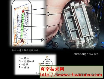
As the “optoelectronic pioneer” in the history of image sensor development, vacuum image tubes established the foundation of modern imaging technology with their unique “energy storage” imaging mechanism. Their core component, the photoconductive target, uses semiconductor materials such as antimony sulfide (Sb₂S₃) and lead oxide (PbO), which exhibit significant photoconductive properties—where conductivity changes with the intensity of incident light, thus achieving the conversion from optical signals to electrical signals. When light passes through the optical system and projects onto the surface of the photoconductive target, different areas form corresponding charge distributions due to variations in light intensity, temporarily storing image information like an “optical memory.” The electron beam emitted by the electron gun scans the photoconductive target in precise timing, converting the optical image into an electrical signal output by reading these charge distributions, a process fundamentally different from the pixel array working principle of modern sensors.
Historically, vacuum image tubes became the benchmark technology in the broadcasting field due to their excellent image quality, widely used in broadcast-grade cameras from the 1950s until the early 21st century. Despite inherent limitations in size, power consumption, and lifespan, their pioneering position in the evolution of image sensor technology is irreplaceable, providing important theoretical and practical references for the subsequent development of CCD and CMOS technologies.
CCD Era
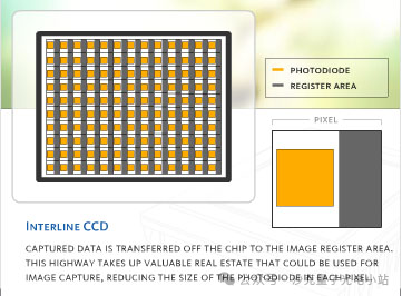
The development of CCD (Charge-Coupled Device) technology exhibits significant technological differentiation in its structural evolution and application expansion. Divided by the dimension of optical signal acquisition, CCDs can be categorized into two main types: line scan CCDs achieve one-dimensional optoelectronic conversion through a single row of photosensitive elements, widely used in image acquisition for scanners, optical signal detection for spectrometers, and push-broom imaging systems for orbital satellites, with imaging principles similar to constructing two-dimensional images through linear scanning; area scan CCDs utilize a two-dimensional photosensitive array to directly achieve parallel capture of spatial light fields, further subdivided into interline transfer (IT) and frame transfer (FT) structures based on differences in charge transfer mechanisms. The interline transfer structure achieves rapid charge transfer by setting opaque vertical shift registers between photosensitive elements, effectively suppressing image smearing; the frame transfer structure separates the photosensitive area from the storage area, demonstrating unique advantages in high-speed photography.
Among the many breakthroughs in area scan CCD technology, back-illuminated technology has set a low-noise benchmark in the field of astronomical imaging. Traditional front-illuminated CCDs have metal electrodes and wiring layers covering the front of the photosensitive elements, leading to approximately 30% of incident photons being absorbed and lost; whereas back-illuminated technology, through wafer thinning and flip-chip processes, allows photons to directly enter the photosensitive layer, increasing quantum efficiency to over 90% while significantly reducing dark current noise. This technological advancement has been milestone applied in the imaging system of the Hubble Space Telescope, where the back-illuminated CCD camera successfully captured high-resolution images of deep-space celestial bodies, elevating human observational precision of the universe to new heights.
However, the physical limitations of CCD technology have gradually become apparent as application demands have upgraded. Analyzing from the device physics perspective, its core bottlenecks mainly manifest in three aspects: first, high drive voltage requirements, where the charge transfer process relies on multi-phase clock signals, with typical operating voltages reaching 12-15 V, increasing system power supply complexity; second, limited readout speed, where charges must be output pixel by pixel through a serial shift register, resulting in a frame rate limit of around 30 fps, which is insufficient for high dynamic scene capture; third, prominent power consumption issues, where continuous charge transfer operations typically cause device power consumption to exceed 1 W, posing serious heat dissipation challenges in portable devices. These structural defects have provided a technological breakthrough for the rise of CMOS image sensors, propelling the image sensor industry into a new development stage.
Rise of CMOS
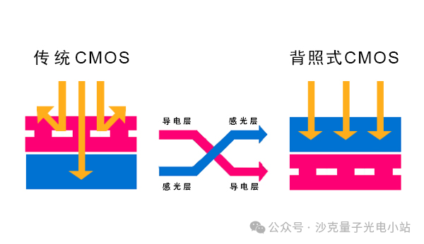
The rise of CMOS image sensors is centered around the breakthrough of pixel-level amplifiers, which utilize a source follower structure to integrate signal amplification functionality within each pixel unit, fundamentally resolving the signal loss and integration bottleneck issues that CCD sensors face due to reliance on external amplifiers. This innovation enables each pixel to possess independent signal processing capabilities, laying the hardware foundation for system-on-chip integration.
In application scenarios, the low power consumption advantage of CMOS is particularly significant, with typical power consumption of only 0.3 W (about 1/10 of the same resolution CCD), combined with on-chip integrated ADC and ISP, enabling smartphone cameras to achieve real-time HDR synthesis and 4K video recording; in the automotive field, its high frame rate characteristics (up to 1000 fps) meet the environmental perception needs of autonomous driving. Specially shaped sensors further expand imaging boundaries, with global shutter pixels solving motion artifact issues, SPAD arrays achieving single-photon level detection, and ToF depth sensors constructing three-dimensional spatial perception capabilities through infrared time-of-flight measurements, driving the development of emerging fields such as AR/VR and robotic vision.
Infrared Thermal Imaging
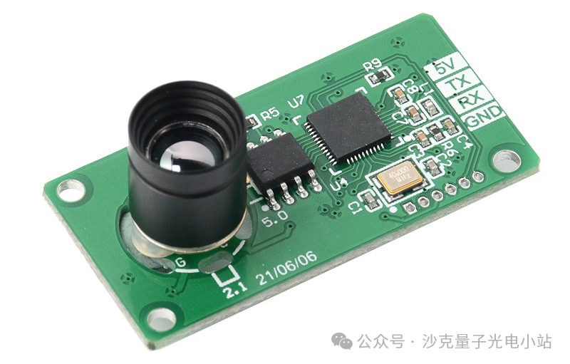
Infrared thermal imaging technology forms a technical branch based on two core sensing principles: uncooled types use vanadium oxide (VOx) or silicon diode micro-radiometers to achieve imaging by sensing temperature changes caused by the thermal radiation of target objects; cooled types rely on materials such as cadmium telluride (MCT) or indium gallium arsenide (InGaAs), requiring operation in low-temperature environments to reduce thermal noise. This difference in technological pathways directly leads to performance differentiation: cooled sensors excel in sensitivity (typically reaching 0.01℃) and resolution, while uncooled types achieve breakthroughs in miniaturization and cost-effectiveness due to the absence of a low-temperature cooling system.
In practical applications, the two types of technologies form a complementary pattern. Cooled sensors are indispensable in high-precision detection scenarios such as semiconductor hotspot analysis, where their high resolution can capture micron-level thermal distribution anomalies; uncooled technology, through material innovations (such as optimizing vanadium oxide thin film processes), has reduced costs to 1/5 – 1/10 of cooled types, promoting large-scale applications in thermal defect detection of electrical equipment and temperature measurement for COVID-19 prevention. For instance, in power inspection, drones equipped with uncooled infrared sensors can identify overheating faults in transmission line joints in real-time, improving efficiency by over 300% compared to traditional manual inspections; during the COVID-19 pandemic in 2020, door-mounted temperature measurement devices based on micro-radiometer arrays achieved non-contact screening with an accuracy of 0.3℃, with daily detection volumes exceeding ten thousand per device.
The popularization of uncooled technology is reshaping the application boundaries of infrared imaging, rapidly penetrating from traditional military fields into consumer electronics, industrial inspection, and medical diagnostics in the civilian market. With the continuous optimization of thermal-sensitive materials such as vanadium oxide and barium strontium titanate (BST), along with the maturity of wafer-level packaging technology, uncooled infrared sensors are expected to further narrow the performance gap with cooled products while maintaining cost advantages, extending thermal imaging technology into broader intelligent scenarios.
Low Light and Image Enhancement
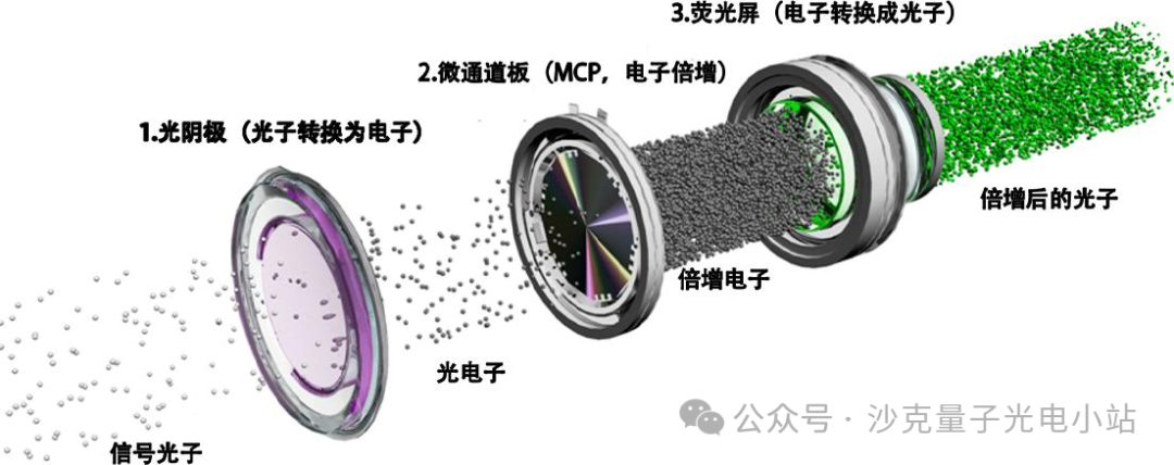
Image enhancers achieve extremely low light imaging through a three-level conversion of “photon-electron-optical signals”: first, the photoelectric cathode converts incident photons into photoelectrons, which are then multiplied through a microchannel plate (MCP), and finally, the enhanced electronic signals are restored to visible light images via a phosphor screen. The core performance parameter, equivalent background illumination (EBI), directly determines the ability to detect extremely low light, with lower EBI values indicating less imaging noise in dark environments. The generational evolution of technology shows significant improvements: Gen-II+ has a 30% increase in sensitivity compared to earlier models, Gen-III has improved quantum efficiency to over 50% by introducing GaAs photoelectric cathodes, while Hybrid CMOS-I² technology has achieved pixel-level integration of image enhancers and CMOS sensors.
Currently, low-light imaging has formed a collaborative system of “physical enhancement + algorithm optimization”. For example, in smartphone “starry sky mode,” multi-frame synthesis suppresses noise and enhances dynamic range, allowing clear star maps to be presented in 0.1 lux environments, supported by the hardware foundation of image enhancers. This technological pathway has been widely applied in scenarios such as vehicle night vision systems (with detection distances increased to 200 meters) and helmet-mounted low-light devices, driving the penetration of low-light imaging from professional military fields into consumer electronics and intelligent transportation in the civilian market.
Technological Turning Points in the Next Decade
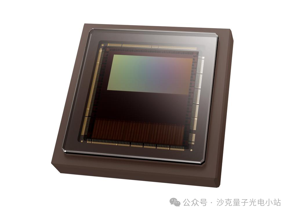
In the next decade, the field of image sensors will encounter multidimensional technological turning points, breaking existing performance boundaries through hardware innovation and interdisciplinary integration. 3D stacked CMOS + SPAD fusion technology vertically stacks single-photon avalanche diode (SPAD) arrays with CMOS readout circuits, physically resolving the inherent contradiction between single-photon sensitivity and high frame rates, allowing sensors to achieve microsecond-level time resolution even in low-light environments, providing foundational hardware support for ultra-high-speed environmental perception in autonomous driving.Neuromorphic vision sensors (Event Cameras) adopt an event-driven imaging paradigm, triggering data output only when pixel light intensity changes, achieving μW-level power consumption and equivalent frame rates exceeding 10 kfps, meeting the dual demands of low power consumption and high-speed response for applications such as drone navigation and industrial inspection.
The integration of on-chip AI-ISP upgrades sensors from mere signal acquisition devices to intelligent perception nodes, enabling real-time intelligent analysis of raw data by embedding neural network processing units near the pixel array. Breakthroughs in quantum imaging technology at the chip level are expected to break the physical limits of traditional optical imaging, providing new observational means for fields such as biological microscopy and deep space exploration. These technological innovations collectively construct a next-generation image sensor technology system that integrates “hardware-algorithm-quantum physics,” profoundly changing the underlying logic of information acquisition and visual perception in the next decade.
The technological evolution of image sensors over the past fifty years has always revolved around the core goal of “breaking physical limits and expanding perception boundaries,” with their strategic positioning as the “core gateway” of the information world becoming increasingly prominent. The technological leap from vacuum tubes to CMOS essentially represents a journey of the collaborative evolution of sensitivity, speed, intelligence, and power consumption—each innovation in the optoelectronic conversion mechanism has propelled humanity’s ability to capture visual information to new heights. This development pattern driven by the understanding of technological mechanisms not only reveals past innovation paths but also provides important insights for predicting future breakthroughs in imaging technology: understanding the essence of the interaction between light and electricity is key to defining the appearance of the next frame of “future imagery.”