This article is adapted from RFsister Maker RF Space.
The development of the Internet of Things (IoT) and smart homes has deepened the interaction between people and objects, making our lives richer, communication more convenient, and connections tighter. The connection between people and objects (devices) relies on wireless networking via the Internet, yet there are many types of connection protocols, such as major categories like WiFi, BLE, Zigbee, and Z-wave, as well as niche ones like NB-IoT and LoRa. Even within the WiFi protocol, there are multiple chip platforms such as Qualcomm QCA4004, MTK’s MT7688, Espressif’s ESP8266, and Realtek’s RTL8710. This inevitably brings challenges to engineers during the early stages of product development: What protocol is suitable for the product? What parameters should be considered? What testing and measurement methods are available?
Today, I will take Realtek’s RTL8710 WiFi module as an example and provide a detailed discussion on the R&D selection and production process, supplemented by the processes of chip packaging, PCB production, and SMT processing, in hopes of clearing the fog to reveal the moon.
The Four Stages from Chip to Module

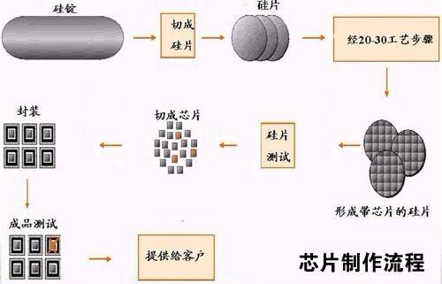
1.Chip (In this stage, I admit my superficiality, so please bear with me~)
Here is a chip production process I found on Baidu, let’s learn together.
Now, let’s focus on the module R&D and production process;
Here is a flowchart with segmented explanations;
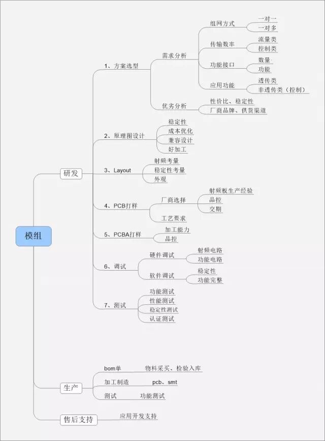
2.Module R&D
This mainly involves hardware design and software design;
As the saying goes, one must plan before taking action. Before designing the module, several aspects need to be considered: solution selection, schematic and layout design, PCB and PCBA prototyping, parameter debugging, and testing; among these, solution selection is the most critical.
1. Solution Selection
The core is to meet functionality, ease of supply, and price matching;
(1) Demand Analysis
Functional considerations: The networking method used by WiFi, whether one-to-one or one-to-many. For terminal products, it is one-to-one, while for gateways and routers, it is one-to-many.
In terms of transmission rate, there are flow types and control types. If the module is used in smart appliance control, a control-type chip like the ESP8266 is preferred; if used in products like routers, a flow-type chip like MTK’s 7620 should be chosen;
Regarding functional interfaces, module developers often consider the number of chip interfaces and supported functionalities, such as GPIO, SPI flash expansion, and I2C interfaces. This is quite understandable; for instance, the RTL8710 IoT WiFi chip has over twenty GPIOs, supporting more input/output devices or more external connections or controls. Similarly, considerations regarding interface functionalities cannot be overlooked, such as this chip’s ability to automatically reduce power consumption to the lowest state when idle and wake from sleep mode when entering working state, significantly reducing product power consumption.
Additionally, in terms of application functionality, developers choose between transparent and non-transparent chip solutions based on their needs.
(2) Pros and Cons Analysis
In addition to analyzing market demand for chip solutions, module developers also need to consider the cost-performance ratio and stability of the chip, as well as the original manufacturer and supply channels;
A good product can be excellent in all aspects, but if the price is excessively high compared to the market, no one will dare to choose it. Of course, one cannot only look at the price; the saying that “you get what you pay for” is very true. If two chip solutions have significant advantages and the superior one is slightly more expensive, it will not deter people from choosing it. Speaking of the stability of chip solutions, this is particularly critical. If a chip has high power consumption that causes overheating and crashes, how can you expect product developers and consumers to choose it? Of course, overheating may be one of many factors causing instability, such as inadequate optimization of software code by the chip manufacturer, which can also lead to the aforementioned issues.
Different manufacturers or brands may offer chip solutions that have their own strengths and weaknesses, or even vary greatly. In the chip industry, there seems to be a consensus that European and American chip solutions are preferred, followed by Japanese and Korean, then Taiwanese, and finally mainland Chinese chip solutions, of course, this is under the premise of similar price differences. While this generalization may not be very scientific, it still holds some reference value. The module chip solutions mentioned above are from a Taiwanese manufacturer.
Finally, no matter how good a chip solution is, if the supply channel is unstable or frequently experiences shortages, it is equally fatal for module developers.
2. Schematic Design
Once the module developer has selected a chip solution, they need to proceed with module development design. The first task in module R&D design is to create the schematic.
Stability: Developers need to design a highly stable schematic based on the chip information provided by the chip manufacturer, according to specification requirements.
Cost Advantage: There are various design schemes for schematics, but cost considerations cannot be ignored. For example, both two-layer and four-layer circuit board designs can be used, but four-layer boards are superior yet more expensive. Of course, this is just one aspect of cost consideration.
Compatibility Design: Electromagnetic compatibility design considerations during schematic design ensure that the module can operate effectively in various electromagnetic environments. The goal is to ensure that the module can suppress various external interferences, allowing it to function normally in specific electromagnetic environments while minimizing its own electromagnetic interference on other electronic devices. Electromagnetic compatibility design considerations involve the stability and performance of the entire module.
Ease of Mass Production: Schematic design must also consider whether it will be easy to process in the future; ease of processing means lower processing costs. If the designed schematic results in a low yield during actual processing, it will also lead to increased costs.
3. PCB Layout
The schematic design mentioned above and the PCB layout are collectively referred to as PCB Layout. The two complement each other; the schematic design must be reflected in the PCB layout, and the PCB layout must consider more factors. For example, RF considerations, stability considerations, structural considerations, and even the aesthetics of the PCB layout. The way the board is designed can indicate whether the module manufacturer is professional.
Of course, the PCB selection involved in the PCB Layout design, such as the types and quantities of resistors and capacitors, will be reflected in the BOM (Bill of Materials), and PCB and SMT production will also be determined according to this list.
4. PCB Prototyping
PCB (Printed Circuit Board) is made of epoxy glass resin material and has different signal layer counts, with chip and other surface-mounted components attached to the PCB.
Manufacturer Selection: For PCB prototyping, module manufacturers typically need to consider whether external manufacturers have experience in module PCB prototyping, whether their equipment meets requirements, and whether their management is solid, etc.
Process Requirements: If the module PCB requires multi-layer prototyping, manufacturers with multi-layer PCB prototyping experience should be sought.
5. PCBA Prototyping
PCBA (Printed Circuit Board Assembly) refers to the entire process of PCB bare board undergoing SMT assembly and then DIP insertion, abbreviated as PCBA, which can be understood as a finished circuit board.
6. Debugging
Debugging the module mainly involves hardware circuit debugging and software debugging.
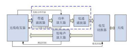
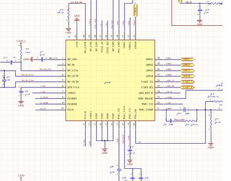
General RF design block diagram for Wi-Fi products
The RF section of a typical Wi-Fi product consists of several major components, with the blue dashed box representing the power amplifier section. The radio transceiver is generally one of the core components of the design, closely related to the RF circuit and typically also associated with the CPU. Here, we will focus on its relationship with the RF circuit. When sending signals, the transceiver itself directly outputs a weak RF signal, which is then amplified by the power amplifier (PA) and radiated into space via the antenna. When receiving signals, the antenna senses electromagnetic signals in space, which are sent to the low noise amplifier (LNA) for amplification through the switch, allowing the amplified signal to be processed by the transceiver for demodulation.
Hardware debugging mainly involves RF circuit and functional circuit debugging. RF debugging includes two major aspects: sending and receiving, with sending involving power and phase error debugging, while receiving includes sensitivity and reception level. Functional circuit debugging focuses more on the debugging of specific hardware function modules.
Debugging RF parameters, for transmission TX mainly involves power, error vector magnitude (EVM), and frequency offset; for reception RX, it mainly involves sensitivity. These parameters affect the stability of WiFi data signal transmission and require specialized instruments for testing, such as LitePoint’s IQ2010 and JDSU’s WT-200. Currently, the RFsister open laboratory provides testing services in these areas.
Additionally, software debugging mainly focuses on stability and completeness of functionality. Generally, only single or partial functions are specifically debugged, and the next step requires more comprehensive testing.
7. Testing
Testing electronic circuits involves a series of measurements, judgments, adjustments, and re-measurements aimed at achieving the circuit design specifications.
Functional Testing: Tests the characteristics and operational behavior of the module based on its supported features, operational descriptions, and user scenarios to determine if it meets design requirements.
Performance Testing: Mainly involves testing various functional circuits of the module, as well as signal transmission distances and other parameters.
Stability Testing: Tests the actual transmission rate, actual power consumption, throughput, and wireless connection stability of the module.
Aging Testing: This is a test conducted to ensure the module’s lifespan and optimal performance during use. Since the system operates for an extended period, it subjects each component to load operation. As long as the performance remains stable under these conditions, the module’s lifespan in normal environments will be extended.
Certification Testing: Certain products must be certified by designated certification bodies in relevant countries, obtaining relevant certificates and affixing certification marks before they can be shipped, imported, sold, and used in service locations, especially for communication products. Common international certifications include FCC (USA), CE (Europe), and RoHS (Europe).
3. Module Production
Module production mainly includes three stages: PCB production, SMT assembly, and module testing:
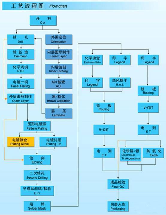
1. PCB Production
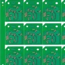
PCB production is the most fundamental and crucial stage of module production. The entire process is illustrated in the following diagram.
The following is a PCB circuit board produced according to module requirements:
 The golden pins are the interface pins.
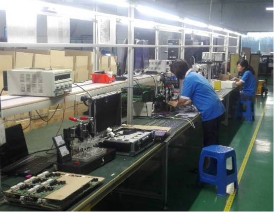
2. SMT Assembly
Based on the characteristics of the module PCB, the module uses single-sided assembly.
Single-Sided Assembly Process
Incoming Material Inspection => Screen Printing Solder Paste (Point Adhesive) => Assembly => Reflow Soldering => Cleaning => Inspection
(1) Material Verification: Before production, it is necessary to verify the specifications and quantities of SMT materials according to the BOM and module production orders;
(2) Machine Adjustment: The SMT machine also needs to be programmed and adjusted, and after the machine adjustment is complete, the material feeding process begins.
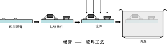
(3) Solder Printing: A suitable amount of solder paste is evenly applied to the PCB pads to ensure good electrical connections between the surface-mounted components and the corresponding pads during reflow soldering.
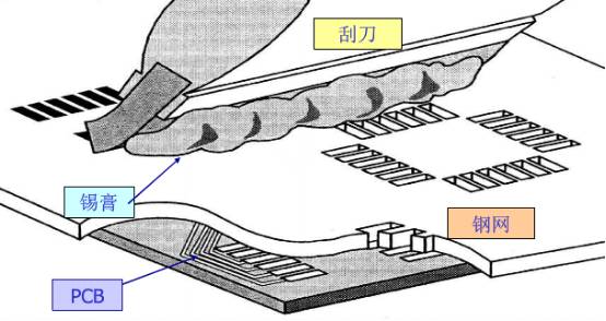 Solder printing illustration
(4) Assembly: The solder-printed PCB is conveyed to the pick-and-place machine for assembly. The pick-and-place machine’s program is pre-written, and when the machine detects the board, it automatically starts picking and placing components.
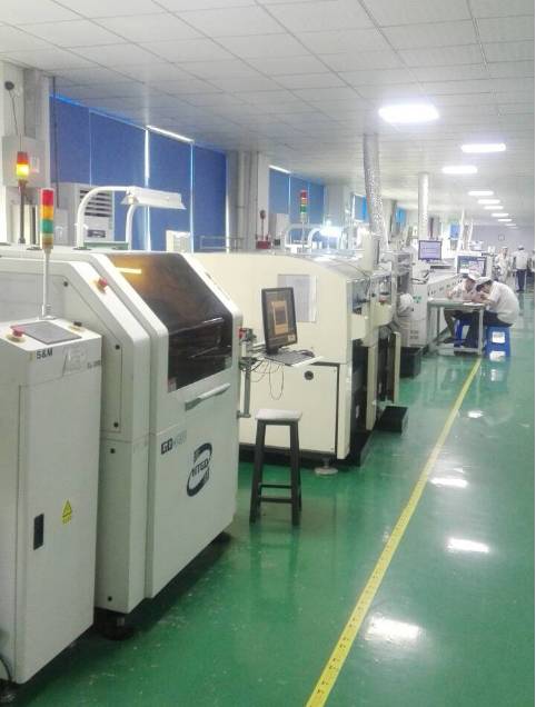
SMT processing line illustration
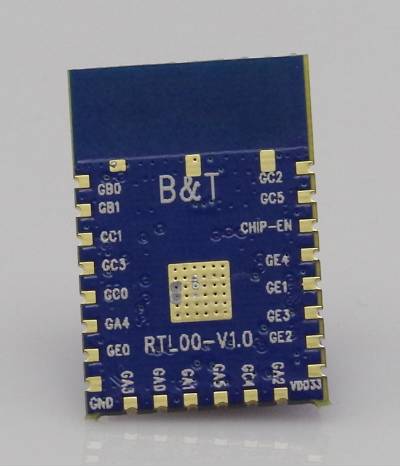
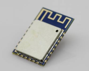
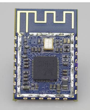 RTL8710 module after assembly
(5) Pre-Reflow Inspection: Also known as Intermediate Inspection, it is important to check the polarity of components, whether the placement is misaligned, whether there are shorts, missing components, or excess solder.
(6) Reflow Soldering: The inspected circuit board undergoes reflow soldering automatically.
At this point, the module production process is basically complete.
(7) Post-Reflow Inspection: Here, the main focus is on checking the appearance of the module for any soldering defects, such as cold solder joints, solder balls, shorts, component misalignment, or standing components. The methods for appearance inspection include: AOI inspection/X-Ray sampling, visual inspection.
A1. AOI Inspection
AOI inspection can typically be performed before or after reflow soldering, but most manufacturers choose to conduct AOI inspection after reflow soldering, as this position can detect all assembly errors encountered.
 AOI inspection
Due to the certain misjudgment (blind spots, insufficient solder, etc.) rate of AOI automatic optical inspection, manual visual inspection is still required after AOI inspection.
 Metal shielding cover on the module
Of course, AOI inspection is a common inspection method after reflow soldering, but since AOI inspection is not feasible for modules with metal shielding covers, we can use another method: X-Ray sampling inspection.
A2. X-Ray Sampling Inspection
X-Ray non-contact 3D inspection method requires higher accuracy for the alignment of inner layers as the number of circuit board layers increases. It can also provide a perspective view of the position and shape of internal components after packaging, and even see through metal shielding devices.
It should be noted that while X-Ray inspection has strong perspective capabilities, it is only a sampling testing method.
B. Visual Inspection
Visual inspection involves scanning the entire board with the naked eye and using a microscope to inspect defective areas, such as insufficient solder, shorts, or twisted pins, which can be adjusted by tilting the board for optimal viewing angles. Checking irregular areas with the naked eye is usually more time-efficient than inspecting them piece by piece with a microscope. Of course, if problems are found, a microscope can be used for more detailed inspection.
 Visual inspection
If problems are found in this stage, the module will be handled according to the situation, including repair, rework, or scrapping.
Next, a laser marking machine will mark the module, allowing us to connect to information about some chip manufacturers, series, and models through the markings on the module.
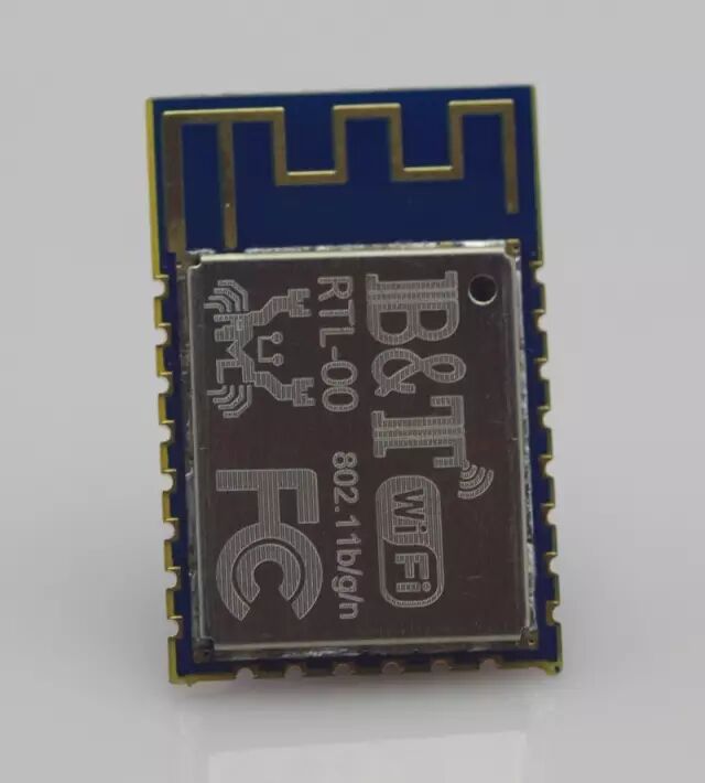
The marking indicates that the module code is RTL-00, it uses Realtek chips, the manufacturer is B&T, and it is a WiFi product compliant with the 802.11b/g/n standard, meeting FCC standards.
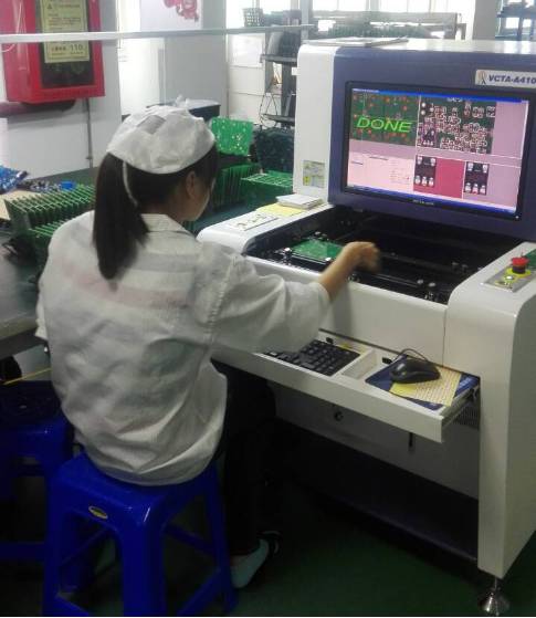
3. Module Testing
(1) Programming
Using a universal serial programmer for programming, first connect the programmer to the computer’s parallel port using a random parallel data cable for online programming.
(2) GPIO Testing
Specialized testing fixtures are used for testing the GPIO ports. The module is placed on a specially designed pin bed fixture, allowing the fixture’s test probes to contact the component leads. By observing the brightness of the surrounding LEDs on the fixture, we can check whether the GPIO interfaces are qualified.
 GPIO testing
(3) Transmission and Reception Power Testing
Using the IQ2010 tester to test the module’s WiFi transmission and reception power.
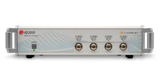 Main testing tools
(4) Others
After testing is complete, the module must also undergo packaging before shipment. In addition to general protective measures against compression and vibration using vacuum foam bags, waterproof and anti-static packaging measures are also important.
Additionally, manufacturers will conduct a certain percentage of random inspections before shipment.
4. Secondary Development Support:
In this service-oriented era, module manufacturers typically provide service support from pre-sales to post-sales, especially reflected in post-sales secondary development technical support.
Commonly used in smart home and industrial control products, WiFi modules are typically embedded. Different fields, products, and engineers may encounter various technical issues during secondary development. Module manufacturers usually provide support through developer communities, technical hotlines, emails, instant messaging, and on-site support services.
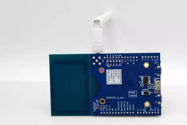
In developer communities, there are usually application development cases, SDK support, firmware update packages, and FAQs. Personally, I enjoy participating in developer communities, not only to communicate with other engineers but also to occasionally share my insights and gain access to some free classic resources. The images of the module in this article (which I obtained from the RTL8710 development community at www.iot-tech-now.com) can be considered a way of giving back.
In Conclusion:
From demand analysis before module R&D to solution selection, from schematic design to PCB layout, from module hardware and software integration to BOM material confirmation; from PCB production involved in module production to SMT processing and testing; from module shipment to post-sales technical support, in every step, we can see the efforts of manufacturers and feel their dedication, rather than just the price you see…