What are the stages of chip manufacturing? First, let’s talk about the manufacturing environment. The chip factory has high requirements for environmental humidity, temperature, pressure, magnetic fields, vibrations, and the number of bacteria indoors. For example, its cleanliness is thousands of times higher than that of an operating room.
Its raw materials, mainly silicon extracted from sand, have a purity level of 99.9999999%, which primarily tests the level of smelting and chemical processing.
Next is the lithography stage, where light behaves as both a wave and a particle, commonly referred to as wave-particle duality. The famous Schrödinger’s cat is related to this concept, and Schrödinger was a scientist who worked in this field. The next concept is wavelength; light is both a particle and a wave, and different light has different wavelengths. You can refer to this spectrum diagram.
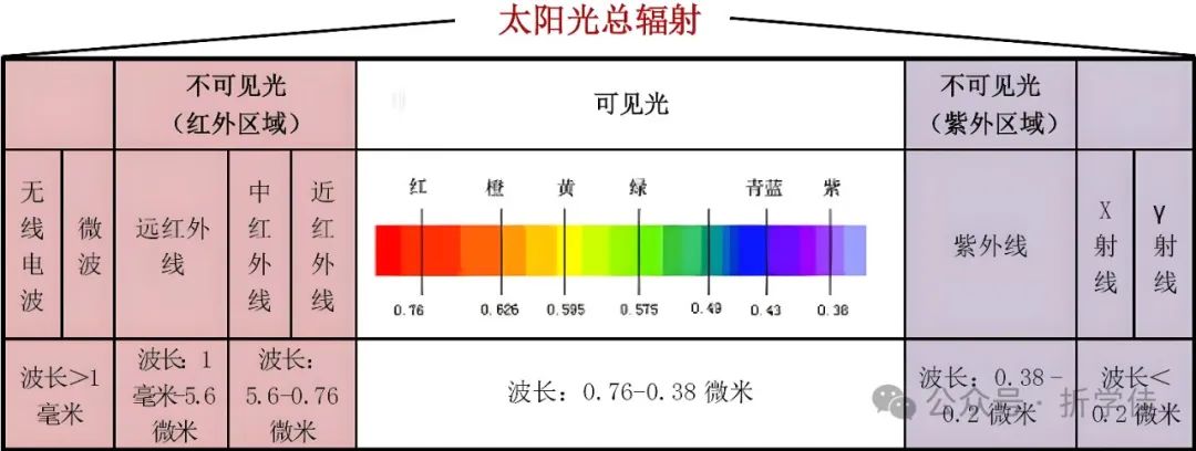
So how does the different wavelength relate to chip manufacturing? Different wavelengths of light etch circuits on the wafer, and the narrower the light wave, the finer the circuit it etches. It’s like using two shovels of different widths to dig a trench; the wider shovel digs a wider trench, while the smaller shovel digs a narrower trench. A narrower trench allows for more circuits to be etched on the same-sized wafer (digging more trenches).

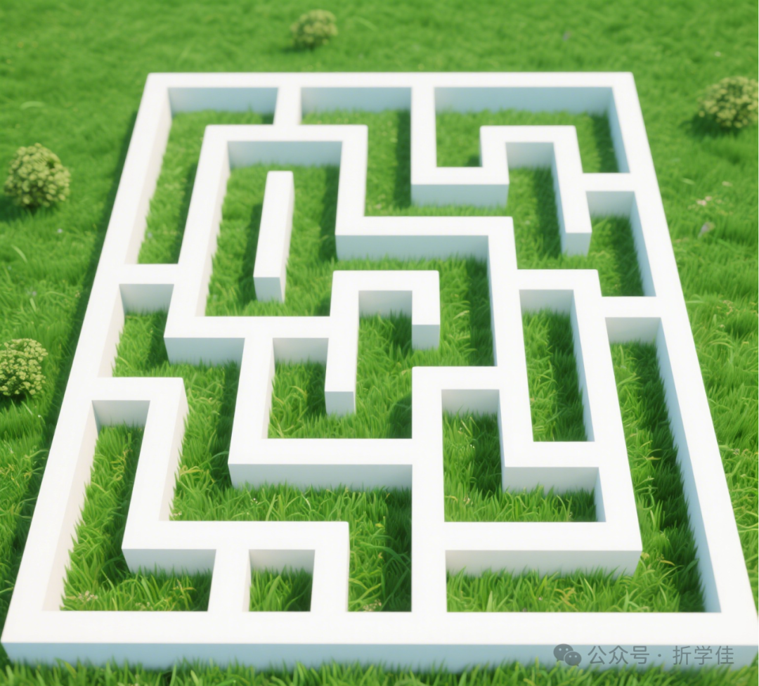
Next is etching and deposition. As mentioned earlier, light etches circuits (digs trenches) on the wafer, but it etches not the silicon itself, but the photoresist coated on the silicon. After etching, washing with chemicals forms a circuit that resembles a maze.
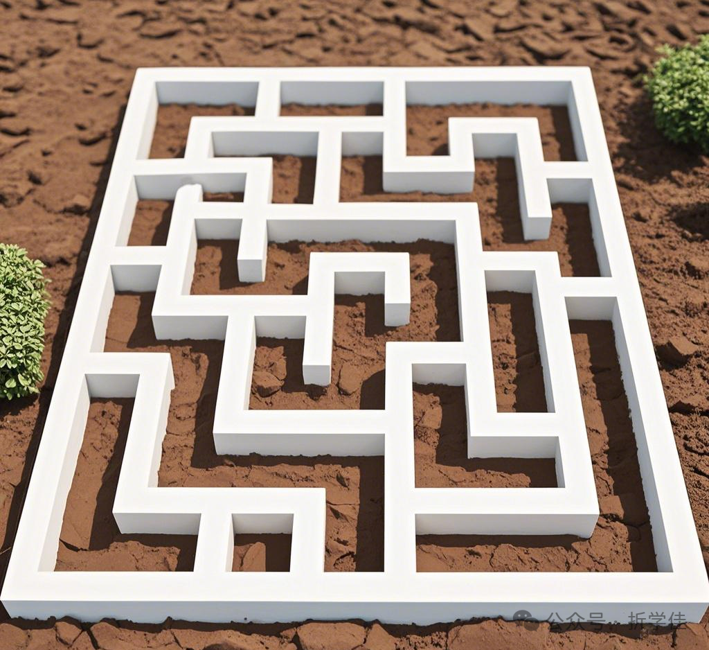
How do we lay down the circuits on the maze paths? Etching is done by using gases or liquids to etch the circuit. After etching, it will remove a layer from the maze paths.
Then, we can deposit the corresponding metal, for example, copper.
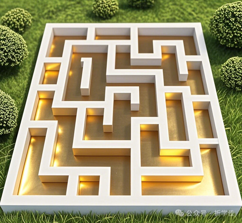
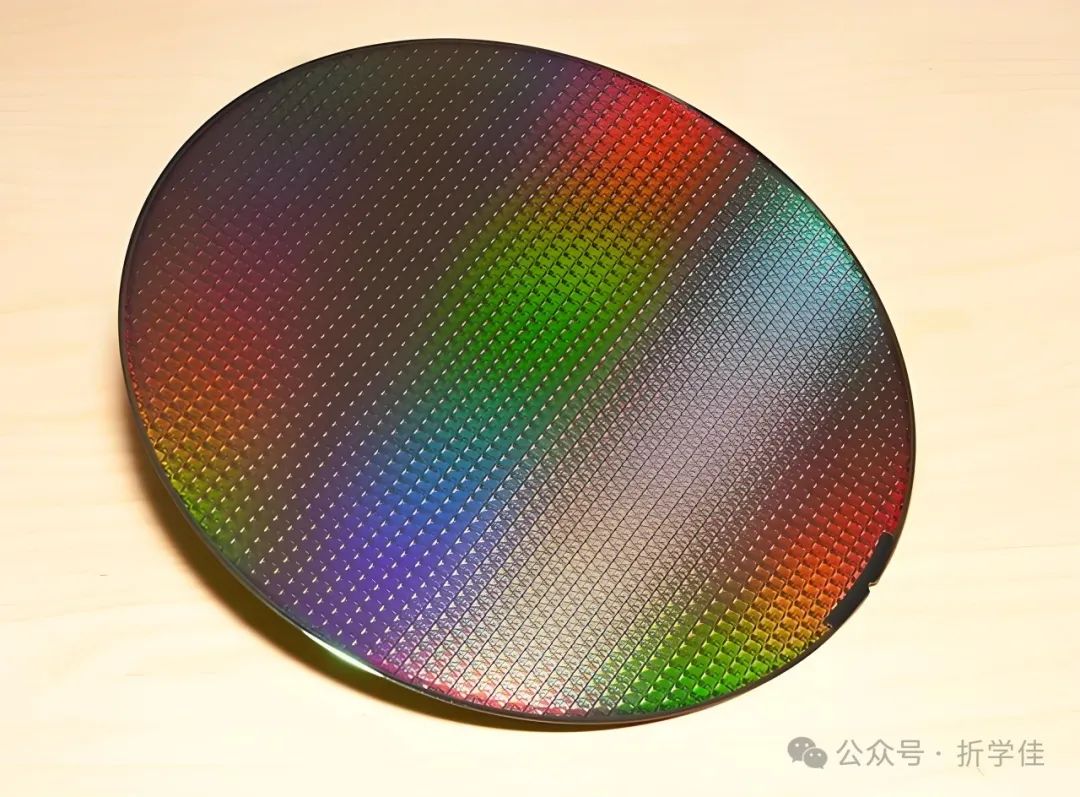
Another method is deposition, which is like directly sprinkling the corresponding metal on the maze. Whether through etching or deposition, after applying the metal on the paths, we wash away the original photoresist with chemicals, forming the circuit. After forming the first layer of the circuit, we reapply photoresist, then proceed with lithography, etching, and deposition, stacking layer by layer. Modern computing chips generally have 70 to 80 layers, while memory chips typically have 200 to 300 layers.
Once all these steps are completed, and after confirming there are no issues during testing, we proceed to the next step: packaging and testing. In simple terms, packaging involves connecting the contact points on the wafer through wiring,
and applying a drop of resin for protection.
This results in individual chips.
The environmental costs account for about 5% of the total cost, lithography accounts for 30%, etching and deposition each account for 25%, and packaging and testing account for about 10%.
The next section will discuss the cost of manufacturing a chip.