In natural convection heat dissipation products, the size of vias on the PCB has a significant impact on heat dissipation. However, the exact extent of this impact is still unknown. We will start with a simple product analysis, focusing on the via parameters of a single chip, to study how changes in via parameters affect the thermal conductivity:
Conditions:
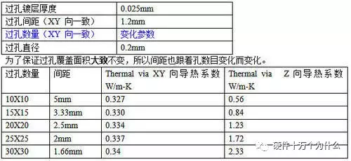
4-layer board, PCB size 100x100x1.6mm, chip size: 40x40x3mm, via range: 40x40mm, via copper plating thickness: 0.025mm, via spacing: 1.2mm, filling between vias: air
For vias, the following parameters mainly affect heat dissipation:
Diameter of the vias, number of vias, thickness of the copper foil in the vias
Of course, manual calculations can also be performed (parallel thermal conductivity):
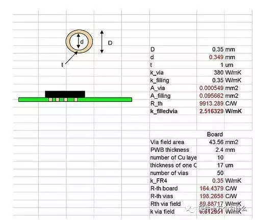
However, since we have software, we can quickly calculate various combinations of changes: 1. The impact of via diameter (other parameters unchanged)
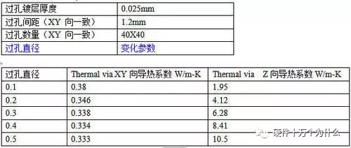
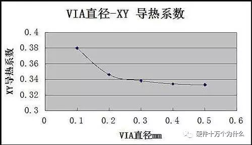
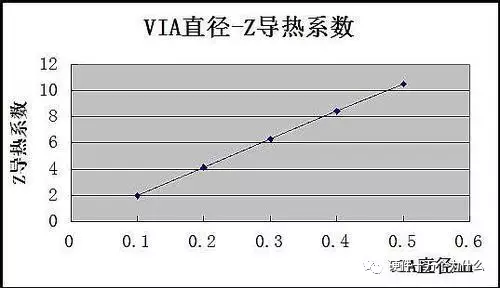
(Why is it linear? Think about it…)
2. The impact of the number of vias (other parameters unchanged)
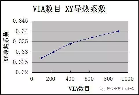
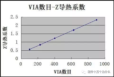
(Also linear…)
3. The impact of copper foil thickness in the vias (other parameters unchanged)
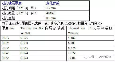
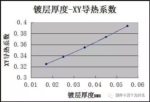
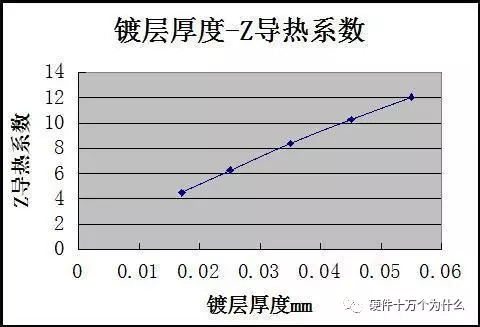
(Still linear…)
Conclusion:
-
The purpose of heating vias is to enhance the Z-direction thermal conductivity, allowing the components on the heat-generating surface to cool quickly. Therefore, based on the above data, it can be seen that increasing the via diameter, increasing the plating thickness, and increasing the number of vias can significantly enhance the Z-direction thermal conductivity.
-
It should be noted that increasing the diameter will impair the XY-plane thermal conductivity, but this impairment can be considered negligible.
-
Additionally, adding filling materials inside the vias can further improve Z-direction thermal conductivity.
-
In natural convection conditions, the heat carried away by convection through the vias can also be considered negligible.
[1]Interest-driven passion
[2]Should hardware engineers design their own PCBs?
[3]How long should PCB traces be??
[4]How wide should PCB traces be?
[5]Inner layers of PCB
[6]Vias
[7]Can PCBs have sharp angles and right angles?
[8] Should dead copper be retained? (PCB islands)
[9]Can vias be placed on pads??
[10] PCB materials, what does FR4 actually refer to?
[11] Solder mask, why is green oil mostly green?
[12]Steel mesh
[13]Pre-layout
[14]Key points of PCB layout and routing
[15]Cross-segment routing
[16]Signal reflection
[17]Dirty signals
[18]Surface treatment processes such as gold plating, tin spraying, etc.
[19]Trace spacing
[20]Placement of capacitors
[21]Crosstalk
[22] Flying probe testing of PCBs
[23]Overview and simulation of FPC
[24] Why do PCBs deform and bend? How to solve it?
[25] Understanding “characteristic impedance” in one article
[26] PCB stacking design
[27] High-speed circuit PCB reflow paths
[28] Power handling and plane segmentation in PCB design
[29] Zigzag PCB routing – Tabbed routing
[30] What is the dielectric loss angle of PCB “∠”??
[31] The impact of PCB copper foil roughness on high-speed signals
[32] Why can’t crystal oscillators be placed at the edge of the PCB?
[33] What are high-speed signals?
[34] What is a transmission line?
[35]Pre-emphasis, de-emphasis, and equalization
[36] How to utilize PCB for heat dissipation
[37]“Stub” in PCB design
[38] Dilemma: Should there be a GND protection line between traces?
[39] PCB copper pouring
[40]Rules to follow when designing PCBs
[41]“Fake eight-layer” in PCB stacking design
[42] Besides stripline and microstrip, there is also “co-planar waveguide”
[43]Parameters related to PCB pad design processes
[44]Why should grounding holes be drilled at the edges of PCBs?
[45] PCBs that are easier to dissipate heat: aluminum substrates
[46]Why should reference planes be hollowed out?
[47] PCB design for crystal oscillators
[48] Designing DC/DC power supply PCBs with EMC considerations
[49] PCB corners, round corners are not necessarily the best routing
[50] Why should vias be plugged? “Conductive via plugging process”
[51]Key points of power PCB layout and routing
[52]Mark points on PCBs
[53]Using ADS to simulate high-speed signal cross-segmentation
[54] Rigid-flex boards (flex-rigid boards)
[55] Mixed-signal PCB design
[56]Placement of capacitors in PCB design
[57] The impact of via stubs in PCB design
[58]Placement and routing of decoupling capacitors in PCB design
[59] PCB design checklist: Structure
[60] PCB design checklist: Power
[61] PCB design checklist: Routing
[62] PCB design checklist: High-speed digital signals
[63] Process edges
[64] PCB design: Gold fingers
[65] PCB design: Differential pairs
[66] PCB design and simulation for DDR4
[67] PCB material properties to consider in circuit board design
[68]What constitutes a good “PDN” in PCB design
[69] Detailed layout and routing design of PCBs
[70]USB2.0 PCB routing
[71] Key points of flyback switch power supply PCB design
[72] PCB design, pad and via process specifications
[73] Factors affecting loss in PCBs
——Recommended Hardware Books——