2025.05.25
Word Count: 3931
Estimated Reading Time: 5 minutes
Abstract
SRIO is commonly used for communication between FPGA and DSP, FPGA to FPGA, and inter-board communication.
Based on previous experience implementing SRIO protocol communication between FPGA boards and between FPGA and DSP in projects, this article shares how to easily develop SRIO applications in FPGA.
This article mainly introduces data communication in the form of NWRITE + DOORBELL. Please message for related code.
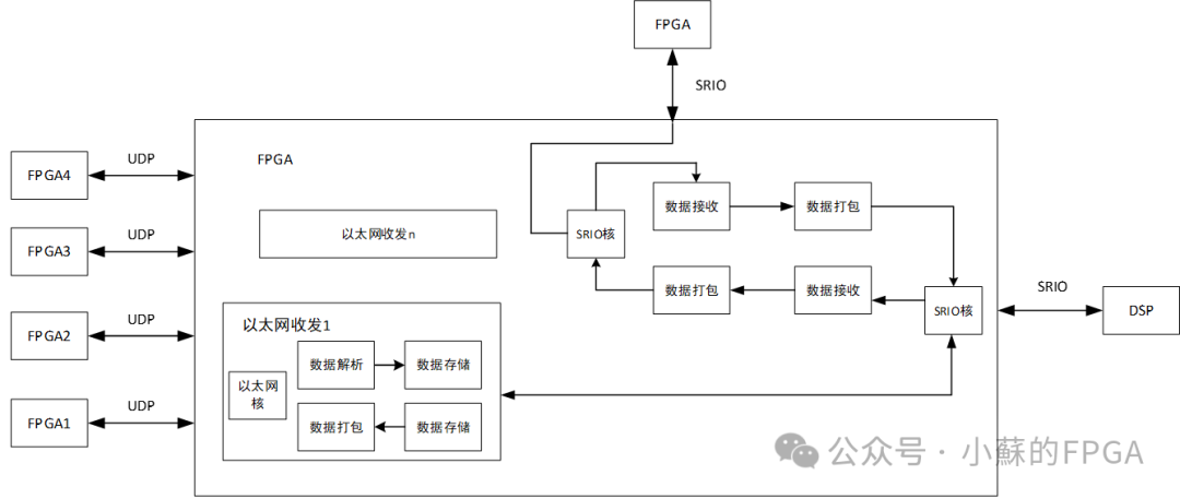
The above image shows a data protocol conversion scheme between multiple FPGAs and DSPs.
1. Overview of SRIO
1.1 Introduction to SRIO
SRIO stands for Serial RapidIO, a high-speed serial communication protocol implemented on the FPGA side based on SerDes, using 8B/10B encoding.
The SRIO protocol consists of a logical layer, a transport layer, and a physical layer.
The logical layer defines the protocol and packet format, such as user interfaces: IO and message interfaces, to achieve communication.
The transport layer contains information related to the data channel: packet switching, routing addressing. For example, it supports 8-bit/16-bit device IDs, accommodating 256 or 65536 interconnected devices.
The physical layer describes the interface protocol between devices, such as flow control, number of lanes, etc.
1.1.1 SRIO Core Framework
The SRIO core framework is as follows:
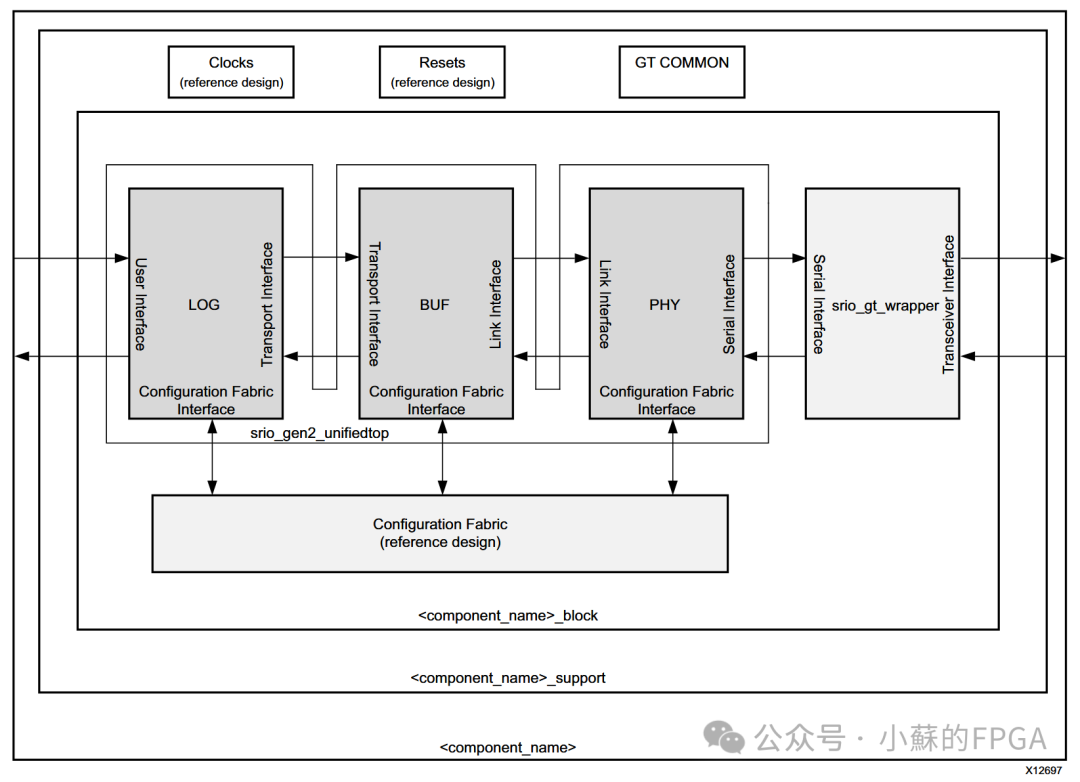
The above image describes the three-layer protocol of SRIO: logical layer (LOG), transport layer (BUF), and physical layer (PHY), as well as the GT interface, clock, and reset relationships. SRIO is encapsulated based on high-speed transceiver GT.The PHY layer frames and deframes data based on GT, and the clock of the PHY layer is related to GT. The clock of the logical layer may differ from that of the PHY layer, buffered through BUF. The clock and reset relationships are the same as those in the GT transceiver core application.
1.1.2 Logical Layer Interface
For developing SRIO protocol communication, the focus is mainly on the logical layer interface, especially the user interface.The logical layer is divided into several parts to achieve data packet transmission and reception. The logical layer has three types of interfaces: user interface, transport interface, and configuration interface, with thick arrows indicating AXI-Stream protocol and thin arrows indicating AXI-Lite protocol.
The transport interface is directly connected to the BUFFER, and the configuration interface is used to configure some register parameters of the logical layer, which is generally not commonly used. The user interface frequently uses IO ports to transmit and receive data, while the other ports are also not commonly used.
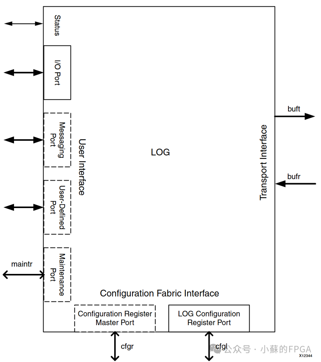
The user interface mainly includes IO port, Messaging Port, Maintenance Port, and User-Defined Port.The commonly used IO port transmits and receives data, while the other ports are not commonly used.
The configuration interface is mainly used for configuring some register parameters, which are not commonly used.
The transport interface includes two ports for sending and receiving, connected to the Buffer, which is not visible to the developer.
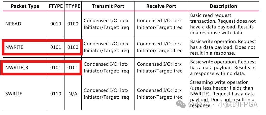
IO port: Common transaction types such as NWRITE, NWRITE_R, SWRITE, NREAD, and RESPONSE (excluding maintenance response), DOORBELL, etc., are all performed on the IO port.Using HELLO or SRIO Stream two data formats, HELLO format is commonly used.
Messaging Port: messages can also be transmitted through IO port (for example, DoorBell can only be on the IO port); Maintenance Port: maintenance data packets require selection for configuring underlying registers; User-Defined Port: custom protocol types.
1.1.3 Communication Transmission and Reception Interface
The commonly used data transmission and reception communication in the user interface is as follows, AXI Stream protocol mode:
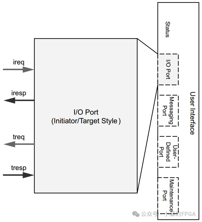
Sending Data: Requests generated by the local device (data sent locally) and doorbells are sent through the ireq channel;
Receiving Sending Response: If the local end sends a transaction with a response (such as NWRITE_R), the response packet generated by the remote device is received through the iresp channel;
Receiving Data: Requests generated by the remote device (data sent from the opposite end) and doorbells are received through the treq channel;
Sending Receiving Response: The response packet generated by the local device is sent through the tresp channel (for example, the local end’s response to NWRITE_R);
1.2 Common Packet Protocols
The packets used for user interface communication include hello packets and stream packets; the timing of hello packets is as follows:
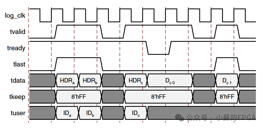
In actual projects, hello packets are the most commonly used, where valid and ready handshakes indicate protocol validity, last indicates the end of the packet, data represents data and header information, keep indicates valid bytes of data, and user contains ID information.
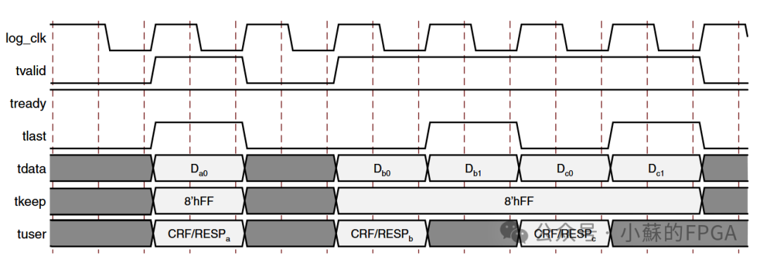
The timing of stream packets is as follows:
1.2.1 Packet Structure
SRIO has three layers: user layer, transport layer, and physical layer, and the corresponding packet structure also has three layers: different fields represent different meanings.
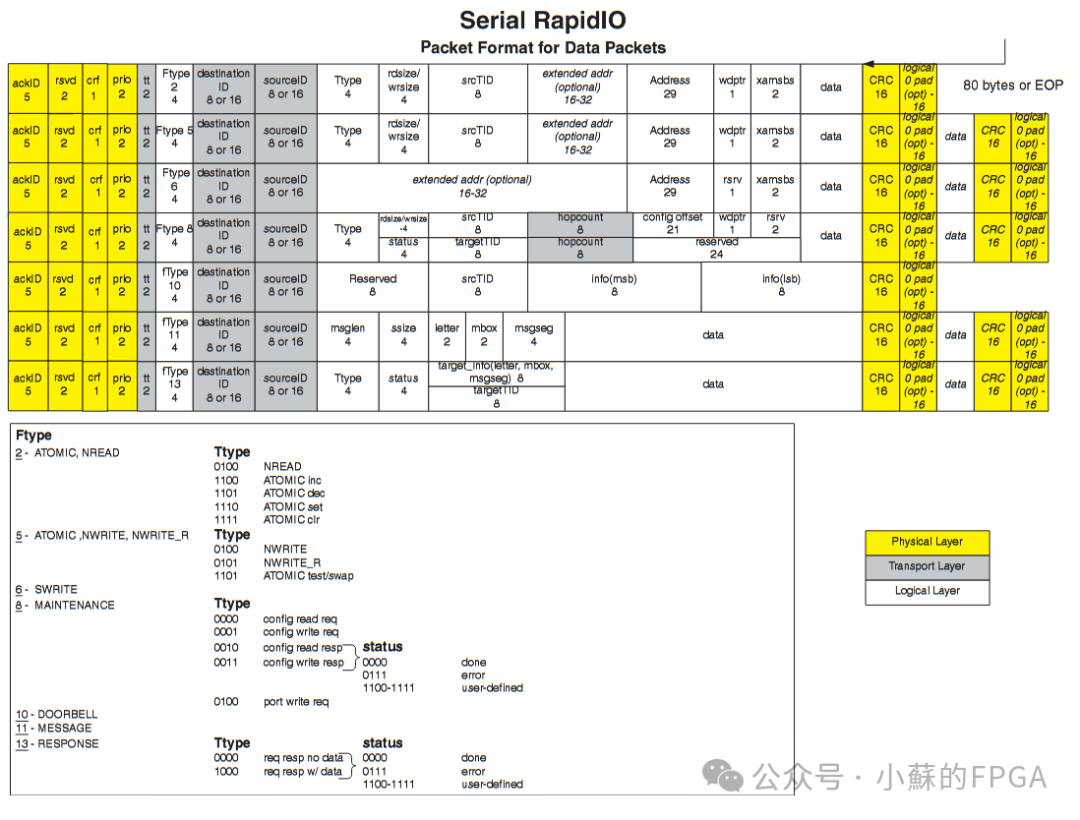
The white part corresponds to the application layer; the gray part corresponds to the transport layer, and the yellow corresponds to the physical layer. For developers, it is necessary to construct and parse the application layer.
Transaction types are mainly determined by Ftype and Ttype fields, commonly used in FPGA are NWRITE, NWRITE_R, DOORBELL, NREAD, RESPONSE (with or without data).
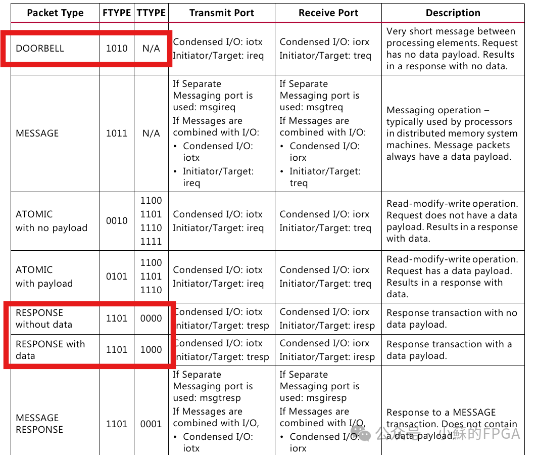
1.2.2 Hello Packet
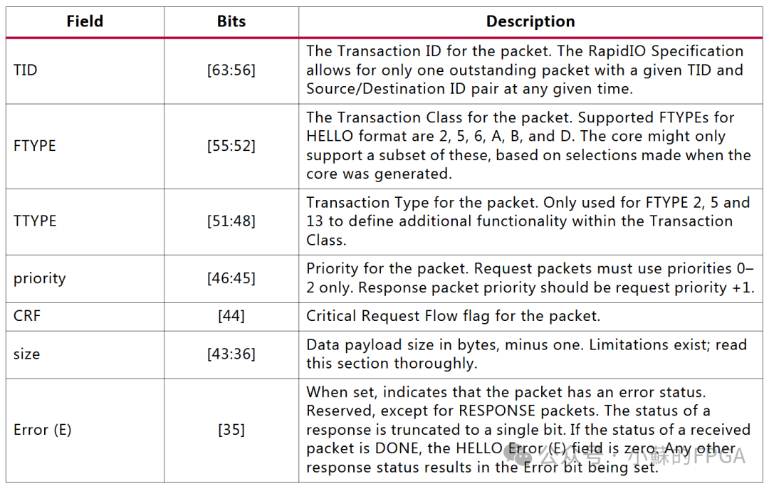
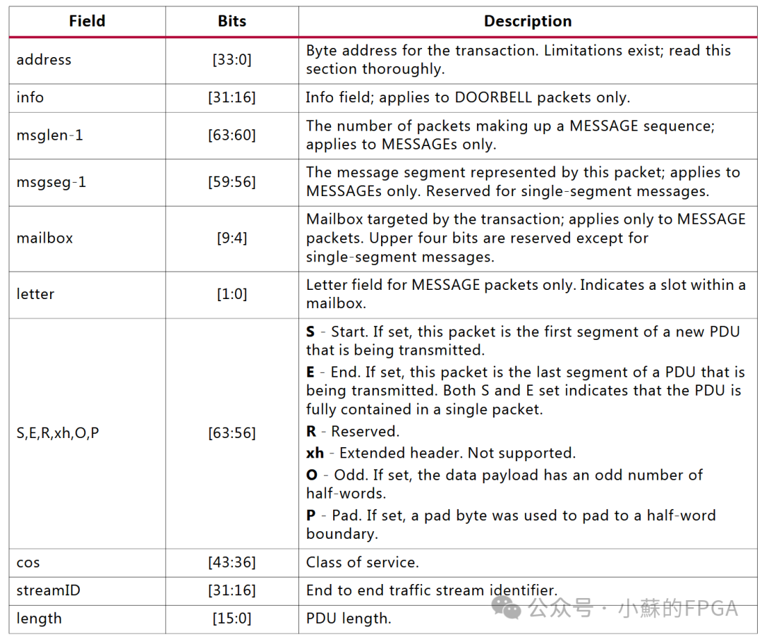
The format of hello packets is as follows: the left red box indicates the transaction type, and the upper yellow box indicates 64 bits, with the list inside representing the meaning of specific positions.In the HELLO data packet format, each clock of the logical layer transmits 64 bits.
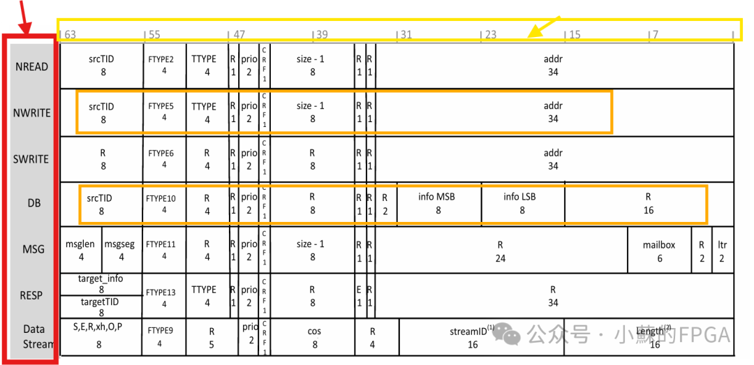
Field meanings: focus mainly on NWRITE and DOORBELL related fields, where size indicates the number of data bytes – 1, with a maximum of 256 bytes per packet; the addr address value must correspondingly change with the number of data bytes per packet. In actual development, each packet’s TID value must be different, and the TID of the DOORBELL must correspond to the last packet’s TID value; otherwise, there is a probability of losing the link.
When valid data is less than 8 bytes or not a multiple of 8 bytes, other control fields are needed to indicate; in practical applications, this situation is mostly avoided, and will not be elaborated here.
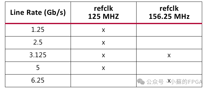
1.3 Clock Relationships
The line rates supported by SRIO and GT reference clocks mainly include the following types: those marked with “x” indicate the types of combinations supported by SRIO.
1.3.1 Clock Framework for Series 7 and UltraScale Series
The clock relationships of SRIO and GT are as follows: Series 7 and UltraScale/+ series
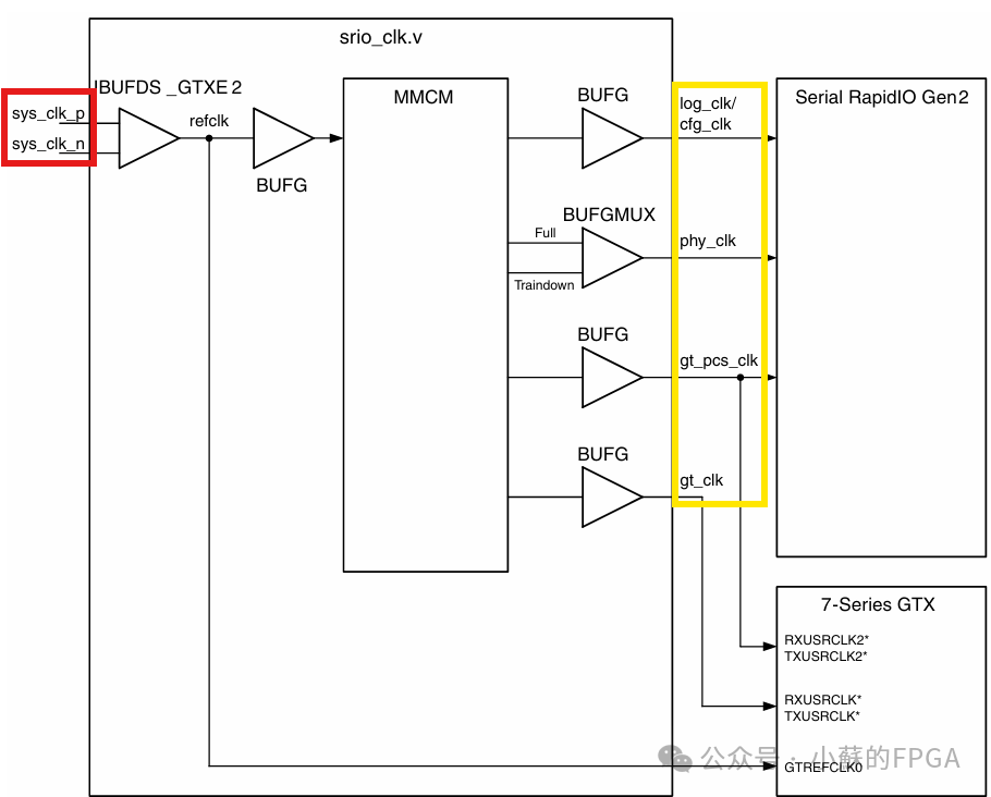
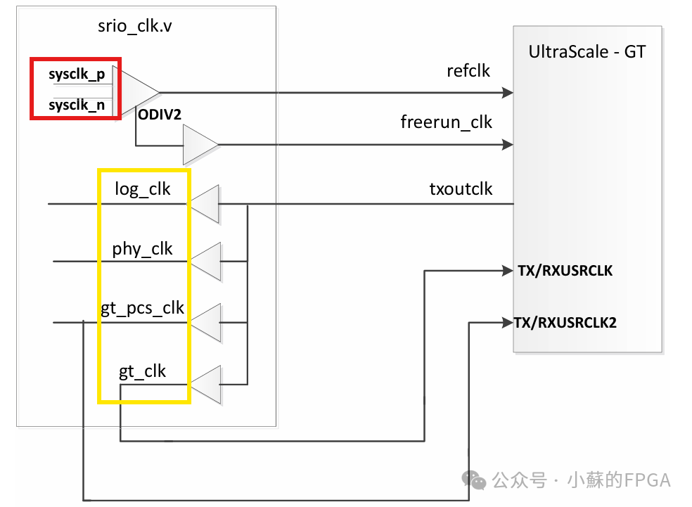
In the above clock framework:phy_clk is the main core clock,gt_pcs_clk is the clock signal for communication between GT and PHY (usrclk2),gt_clk is the clock signal for parallel data of GT’s PCS and PMA (usrclk).log_clk is the clock for data, configuration, etc., of the SRIO logical layer.cfg_clk is the clock for the SRIO configuration interface, which is the same aslog_clk clock.
gt_pcs_clk’s clock frequency = gt_clk/2 (usrclk2 is half of the usrclk frequency),phy_clk=(gt_clk * number of lanes)/4. To prevent BUFFER overflow,log_clk should not be less than phy_clk, and log_clk and phy_clk should be synchronized.
1.3.2 SRIO and GT Clock Relationships
The number of lanes and line rates supported by SRIO mainly include the following categories:GT numbers, x4, x2, x1 three modes.
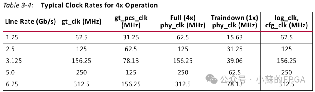
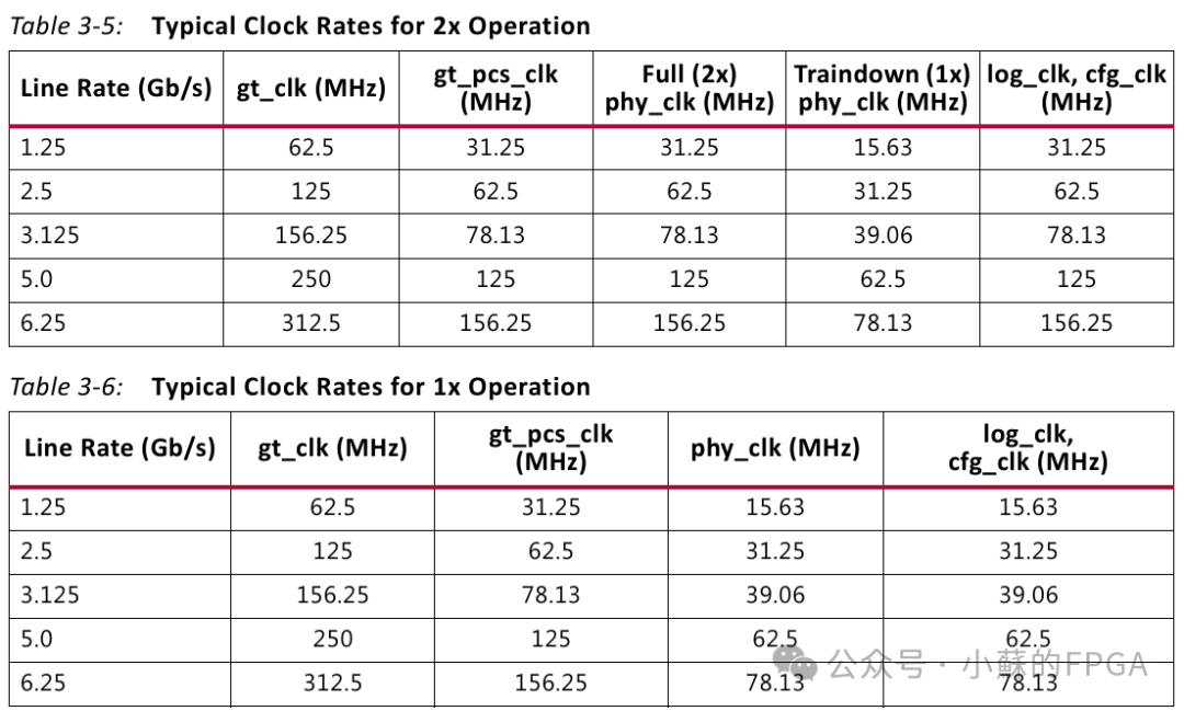
In the above table, without using the Train down function,phy_clk clock frequency equals log_clk
In GT, the parallel data bit width = line rate/usrclk=line rate/gt_clk=20bit, 8/10B conversion, the actual data bit width is 16bit.usrclk2 is half of the usrclk frequency,PHY transmits data once, while GT needs to transmit data twice.
According to the user layerlog_clk/phy_clk once transmits 64 bits, in GT, usrclk2 (gt_pcs_clk) the number of times this data is transmitted can derivethe frequency relationship between gt_pcs_clk andlog_clk/phy_clk.
1.3 Reset
For the use of reset, refer to the reset usage method in the SRIO core example design.Each clock domain has a corresponding reset signal, and the reset signal must be pulled high for at least four clock cycles in the corresponding clock domain to be effective.
2. Using the SRIO Core
Since my development board only has one QSFP optical module single core, and the GT reference clock is 156.25MHz, for ease of testing and verification, this setup uses x4 mode, with a line rate of 3.125Gbps or 6.25Gbps.
2.1 SRIO Core Setup
This design example does not involve the maintenance port, and the mode selection is Basic
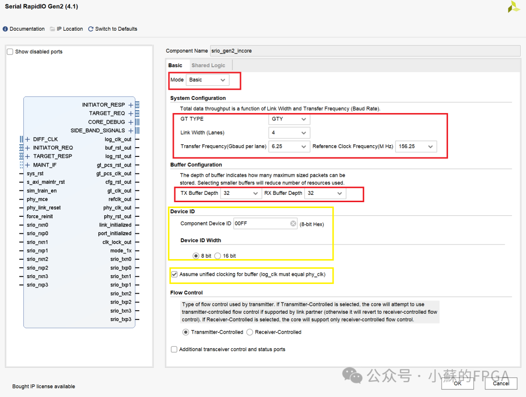
The GT type depends on the FPGA model, which is automatically selected by Vivado;
Lane rate and number, reference clock selection: set according to your development board. Since my development board has QSFP and 156.25MHz, I chose 4 lanes, and the reference clock is set to 156.25MHz. Under this limitation, the line rate has two options: 3.125Gbps and 6.25Gbps. In this simulation, I used a line rate of 3.125Gbps, while for board testing, I chose 6.25Gbps.
Buffer depth can be selected as 8, 16, or 32, and it is recommended to choose 32 for more margin.
Local ID: ID bit width and specific value.
Since this design does not involveTrain down, you can checkphy_clk clock frequency equals log_clk.
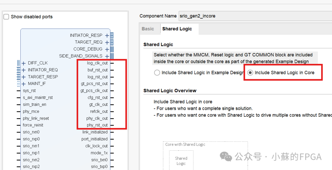
Finally, regarding resource type selection, since on my development board this part of the GT clock is only used by SRIO, there is no sharing of clock resources with other GTs, it can be selected as internal to the core.
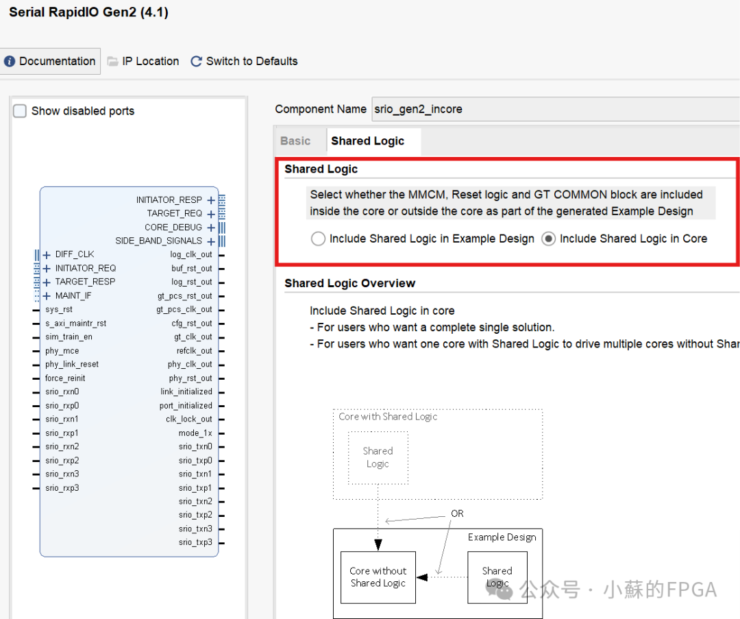
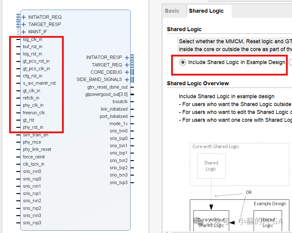
2.2 Core Clock Resource Sharing
This part mainly concerns the use of GT clocks, whenGT clocks are used by multiple different GTs, clock resources need to be shared, selecting one type to share within the core, while the remaining selections are in Example Design; connect the corresponding clocks and resets opened in Core toin Example Design.
3. SRIO Communication Program Design (NWRITE + DOORBELL)
Based on practical application scenarios, the NWRITE + DOORBELL application is widely used, with DoorBell serving as a communication interrupt. One NWRITE carries 256 bytes of data, and in practical applications, if less than 256 bytes, zero padding can be applied.
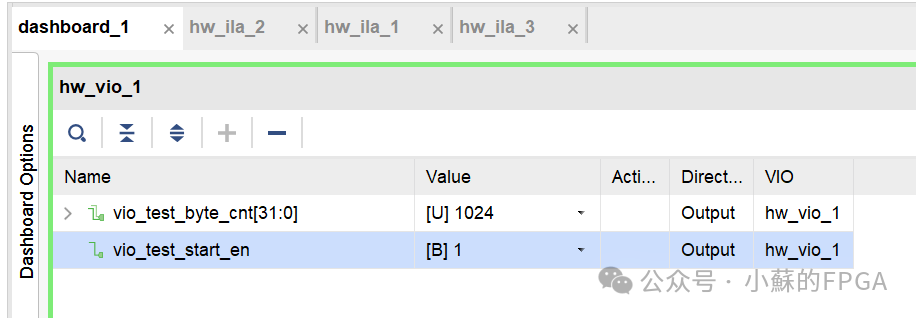
Test scenario: QSFP performs self-loopback testing; VIO control testing can be set to the number of bytes sent in one communication, automatically padding to 256 bytes if not a multiple of 256 bytes, with test data being incremental numbers, and finally sending DOORBELL.
3.1 Test Control Module
Test module: generates test data based on VIO information, controls writing to the test data FIFO; and combines with the ireq module state to control reading FIFO data and the information needed to encapsulate the Hello packet.
Parameter information: port ID, data address, doorbell information.
Port information: link status, nwrite status; output hello packet header information, data, and sending triggers, etc.
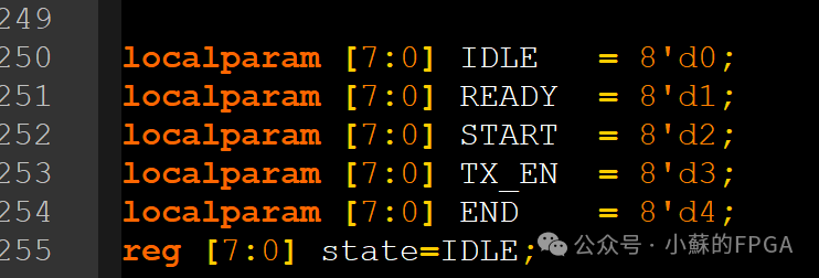
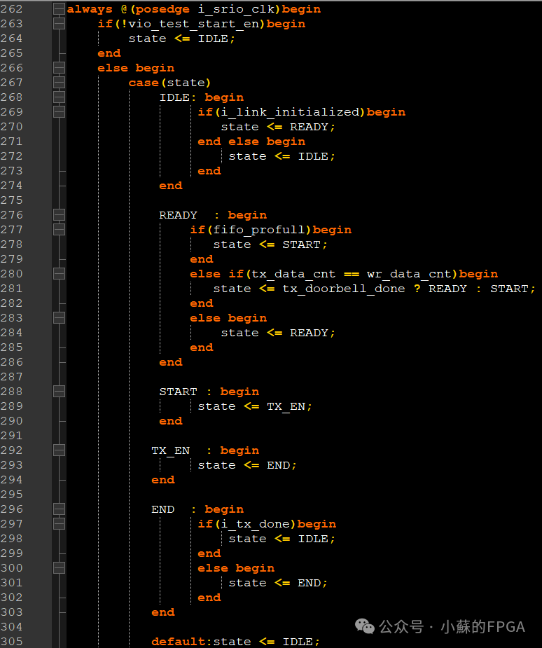
State machine for test data:
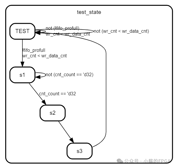
Regarding NWRITE and DOORBELL related information and control states mainly involve:
3.2 Hello Packet Encapsulation Module
The sending of Hello packets occurs at the ireq interface, which mainly encapsulates the NWRITE and DOORBELL packets. The port information is as follows:
The input comes from the test control module, and the output corresponds to the SRIO core’s axis_ireq interface. The state machine design is as follows: a delay is added between nwrite and doorbell; if not added, the doorbell and the last nwrite packet will be back-to-back.
3.3 Hello Packet Parsing Module
Mainly parses NWRITE and DOORBELL information based on Hello packet timing and different field meanings.
The input comes from the axi_treq interface sent from the opposite end, and the output response signal (which can be optionally sent to the SRIO core’s tresp port) receives the NWRITE data and address information and DOORBELL information.
3.4 Link Self-Reset Function
When a link drop is detected, a reset signal of at least 4 clock cycles must be generated to reset the SRIO core; otherwise, it may cause abnormal state signals in the SRIO core, leading to communication failure.
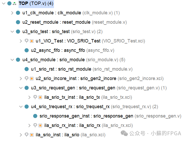
3.5 Overall Project
The structure of the test project is as follows:
4. Simulation Testing
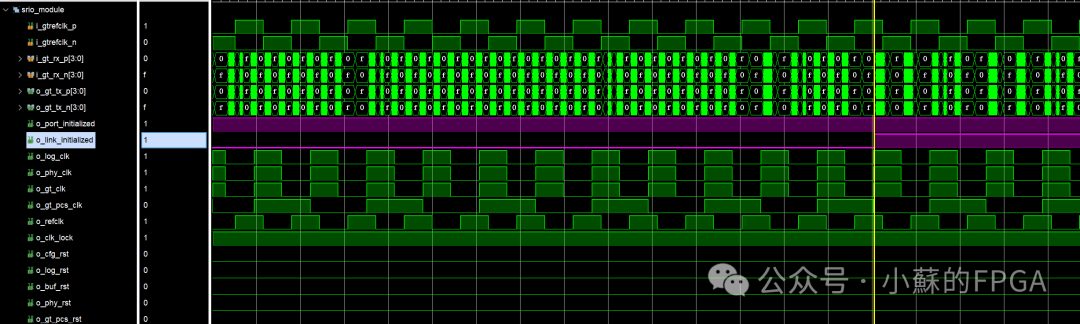
Simulation testing makes it easy to observe many detailed information; the simulation uses 3.125Gbps x4 mode.
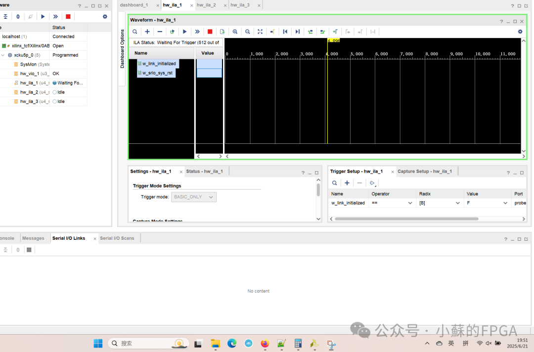
The link establishment process is as follows:
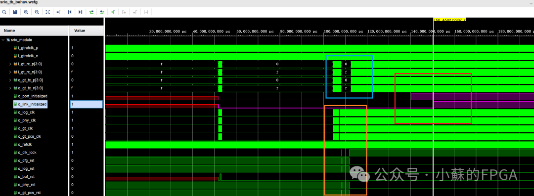
From the above image, it can be seen that the port_initialized signal and link_initialized signal are raised in sequence, indicating that the port and link have been successfully initialized.
The lower part indicates the clock and reset relationships before the link is established.
Only after the link is successfully initialized can SRIO be used for communication.
The clock relationships are as follows: frequency and phase relationships correspond to the datasheet.
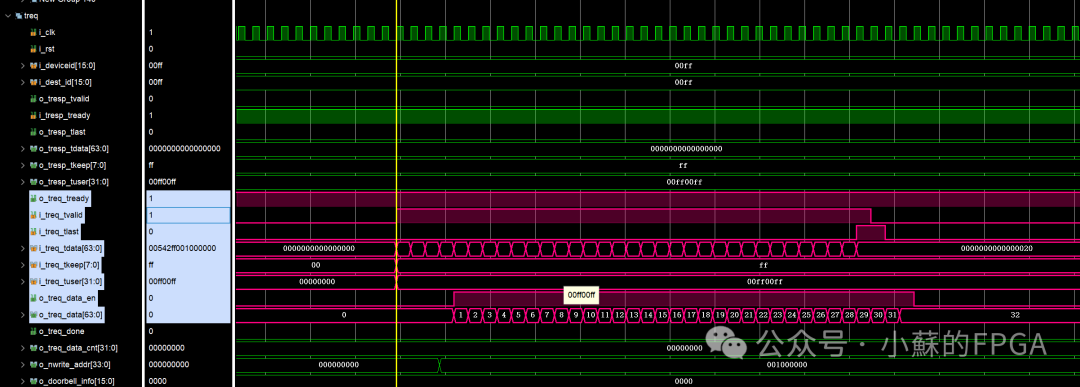
The transmission and reception process of NWRITE + DOORBELL is as follows: 4 NWRITE + 1 DOORBELL
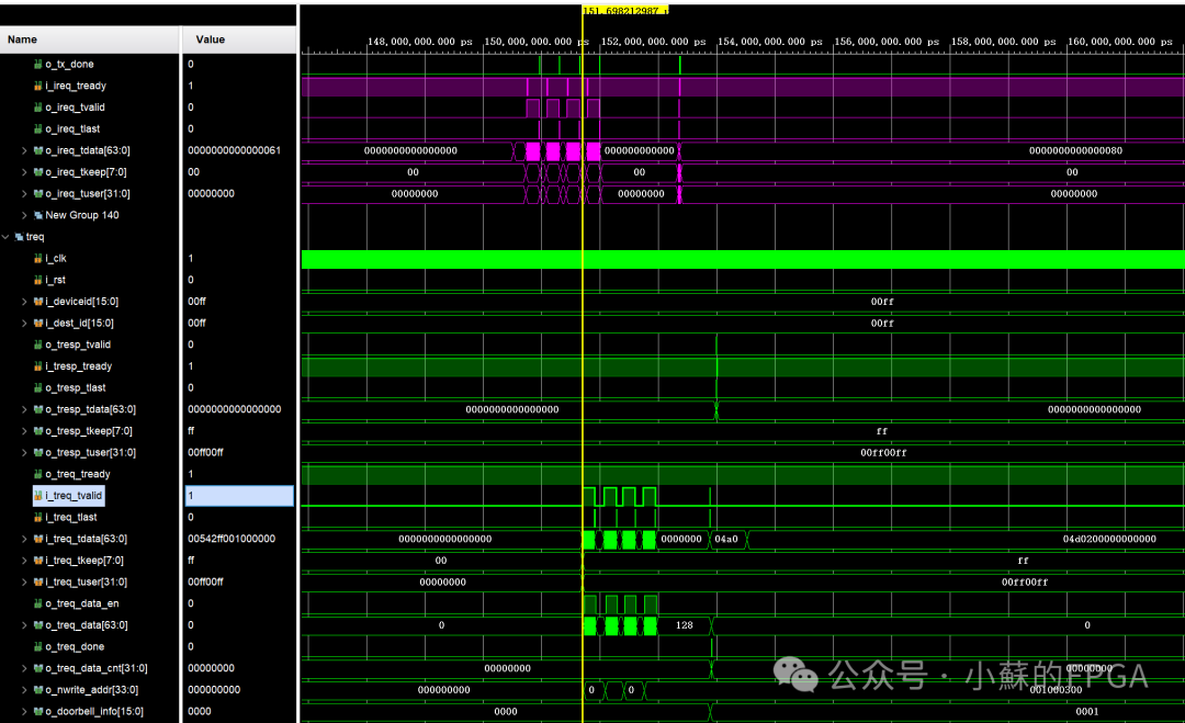
The first and second packets sent are as follows:


The above hello first packet indicates that the address information is 0x001000000,0x001000100, with the protocol type combination being NWRITE
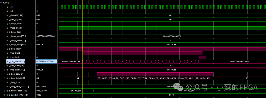
The first and second received packets are as follows: unpacked data is incremental numbers, unpacking is correct.
The sent DOORBELL is as follows: the hello packet header information will not be elaborated.

Input comes from the axi_treq interface sent from the opposite end, and the output response signal (which can be optionally sent to the SRIO core’s tresp port) receives the NWRITE data and address information and DOORBELL information.
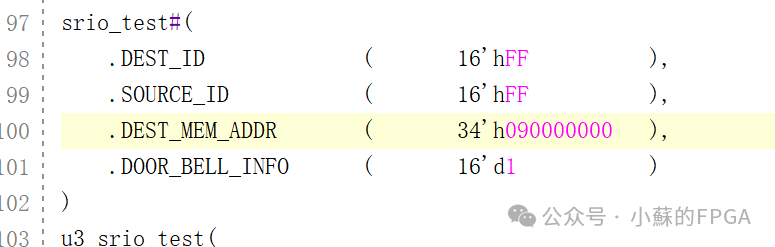
5. Board Testing
Setup information as follows: starting address and doorbell information. Since it is a self-loopback, the transmitter device ID is the same as the core settings.
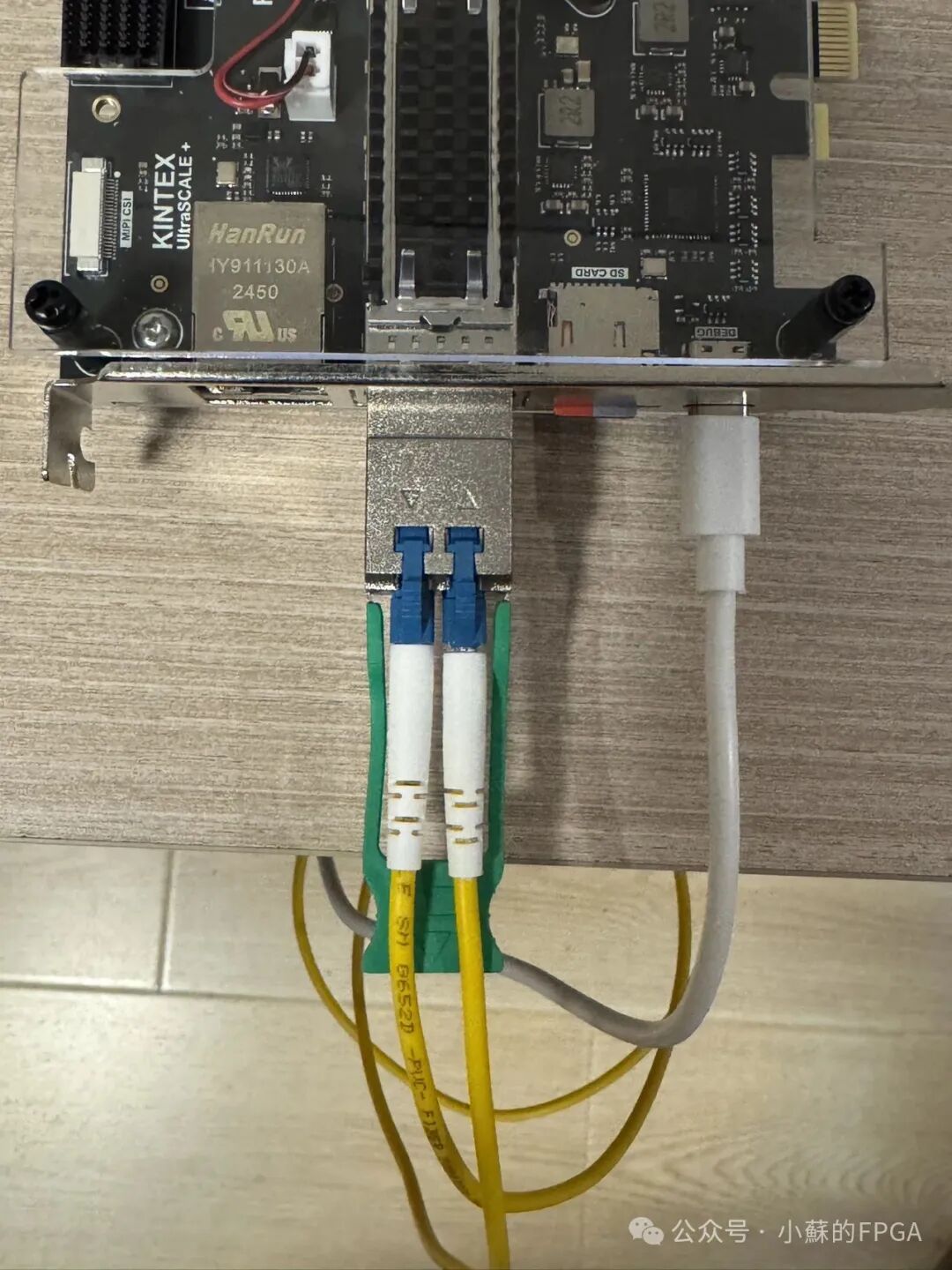
The hardware platform is as follows:
5.1 Link Stability Testing
After powering on, using link drop as a trigger, observe for 10 minutes, the link status is stable.
5.2 Packet Sending Test
VIO sets the number of packets and enables: data size 1K bytes
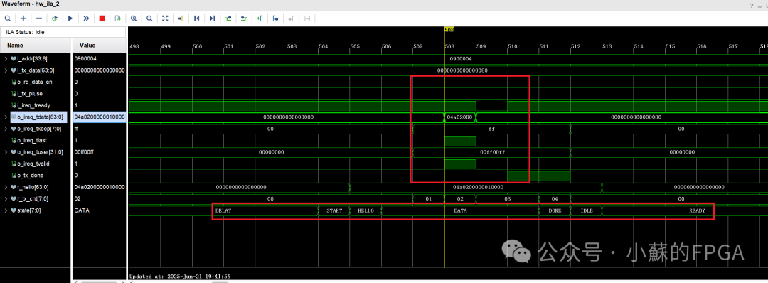
The overall information of 4 packets NWRITE and DOORBELL is as follows:
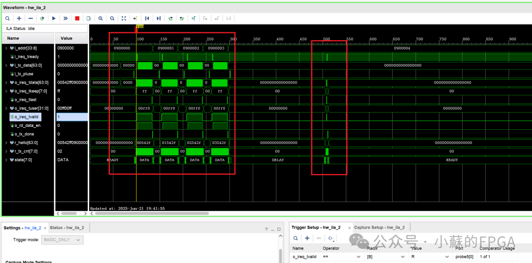
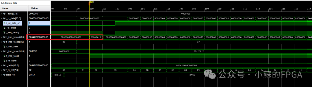
From the above image, the address of each packet, related control information, and status can be obtained. The details of the hello header of the first packet are as follows:
The DOORBELL packet information is as follows: header information, timing, state machine transitions.
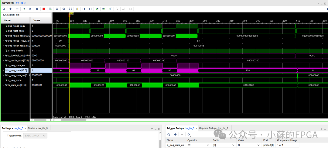
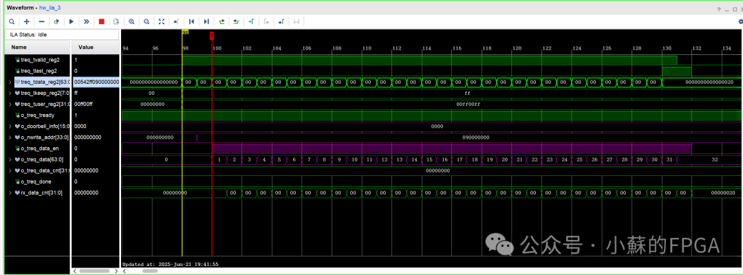
5.3 Packet Receiving Test
The received ILA information: 4 nwrite and 1 doorbell. The doorbell information is 0x0001, and the address information of each packet corresponds to the sent packets.
The first packet information: data is incremental numbers from 1 to 32, parsed correctly.
END
 Previous Issues Highlights ReviewFPGA Implementation of SD Card File Read and Write Function (FAT32 File System)FPGA Implementation of Gigabit Ethernet UDP Protocol (Including ARP, ICMP)Xilinx DDR4 MIG IP Core AXI Interface: FIFO ApplicationRemote Update Function Based on ZYNQFPGA Implementation of Aurora Optical Communication ApplicationXilinx PCIE Data Interaction Application (XDMA)FPGA-Based USB3.0 Usage (CYUSB3014)FPGA-Based Ethernet Flow Control Technology ImplementationMulti-phase DDS Waveform Generation Project ApplicationBroadband Signal Multi-phase Filtering and Pulse Compression Processing (FPGA + ADC)