In today’s global wave of automotive intelligence and electrification, the stability and safety of each electronic control unit (ECU) “brain”—the automotive-grade microcontroller unit (MCU)—has become a top priority concerning life safety.

Chip validation, a crucial yet often overlooked process that is time-consuming and labor-intensive, is the core defense line ensuring the reliability of ECU applications. It spans the entire lifecycle of chip development, accounting for over 60% of development costs, and serves as the ultimate guardian of automotive-grade MCU quality and safety.
1. Automotive-grade Validation: Exceeding the Stringent Challenges of Consumer Electronics
Automotive-grade MCUs are not merely an upgrade of consumer-grade chips. Automotive electronics must face extreme environments (from -40℃ to 150℃+), a lifespan requirement of over 15 years, near-zero fault tolerance, various testing environments as per AEC-Q100, and the dual stringent standards of functional safety (ISO 26262) and information security (ISO/SAE 21434).
Unique challenges of automotive validation:
-
Harsh environments: Electromagnetic interference (EMC), power fluctuations, extreme temperature and humidity cycles, etc.
-
Long lifespan: Aging under ultra-long standby and operational lifetimes, data retention capability validation.
-
Safety first: Systematically preventing, detecting, and controlling random hardware failures and systemic failures.
-
Real-time reliability: Hard real-time response, task execution must be precise and predictable.
-
Zero tolerance for defects: Extremely low defect rate targets (DPPM typically required to be 0).
2. Automotive MCU Validation System: Building a Multi-layer Defense Fortress
In the face of these challenges, a meticulous, multi-layered, and multi-dimensional validation strategy is indispensable.
1. Basic Validation Layer: A Solid Foundation from Micro to Macro
(1) IP-level validation: Comprehensive functional, performance, and boundary condition testing for IP modules such as CPU cores, buses, memory, and peripheral interfaces (CAN FD, UART, SPI, I2C, ADC). Formal verification is widely applied at this level, striving for mathematical completeness.
(2) Subsystem-level validation: Validation of interactions after IP module integration, such as storage subsystems (Cache, SRAM, Flash controller collaboration), power management domains (switching and waking from different low-power modes), and multi-core communication mechanisms. Hardware acceleration platforms often play a significant role at this stage, enhancing the efficiency of complex scenario simulations.
(3) Chip-level validation: Full-chip integration testing. Core tasks include:
-
Functional completeness: Covering all functional points defined in specifications.
-
Performance compliance: Meeting hard metrics such as clock frequency, bandwidth, and latency.
-
Low power validation: Accurate measurement and validation of power consumption in various operational and sleep modes.
-
Clock reset validation: Thorough checks of clock domain crossing (CDC) and reset domain crossing (RDC) to ensure no metastability risks.
-
Register configuration: Validation of read/write, reset values, and bit-field functionality for all software-configurable registers.
-
Firmware co-validation: Introducing real or virtualized models to run low-level drivers and basic software for hardware-software co-validation (HSCV).

2. Automotive-specific validation: Facing extremes and failures
(1) Physical electrical characteristics validation:
-
Static timing analysis (STA): Ensuring setup/hold times meet requirements under all process corners (PVT conditions) without timing violations.
-
Signal integrity/power integrity (SI/PI): Analyzing high-speed signal quality (reflection, crosstalk), power network voltage drop (IR Drop), and ground bounce to ensure reliable signal transmission and stable power.
-
ESD/Latch-up: Strictly following AEC-Q100 requirements, conducting ESD tests such as Human Body Model (HBM), Machine Model (MM), and Charged Device Model (CDM), as well as latch-up effect testing.
(2) Reliability and lifespan validation (AEC-Q100 core):
-
High-Temperature Operating Life (HTOL): Long-term operation (typically over 1000 hours) at 125℃ or higher to accelerate aging simulation of long-term use.
-
Temperature cycling (TC): Rapid temperature change cycles between -55℃ and 150℃ to test the mechanical stress tolerance of chip structures, solder joints, and material interfaces.
-
High-Temperature High-Humidity Reverse Bias (HAST)/Non-Bias (THB): Testing in high humidity (85%RH+) and high-temperature (e.g., 130℃) environments to assess moisture ingress and electrochemical corrosion risks.
-
Solderability testing: Ensuring chip packaging meets subsequent SMT soldering process requirements.
-
Electromigration (EM) and Hot Carrier Injection (HCI) analysis: Simulating and predicting the degradation of metal interconnects and transistor gate oxide layers under long-term current stress.
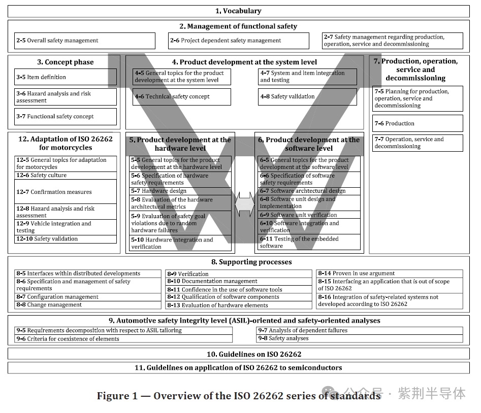
 (3) Functional safety validation (ISO 26262):
-
Safety mechanism validation: Thorough effectiveness testing of hardware-embedded safety mechanisms (such as ECC/parity, watchdog, dual-core lockstep, redundant logic, voltage/frequency/temperature monitoring, bus protection units, memory protection units). This is not merely formal; it is quantitatively assessed through extensive fault injection experiments:
-
Fault Injection: Intentionally injecting hardware faults (Stuck-at, Transient, Delay, etc.) in simulations, FPGA prototypes, or dedicated hardware platforms to verify whether safety mechanisms can timely and correctly detect and handle them, triggering a safe state.
-
Safety mechanism effectiveness assessment: Calculating Single Point Fault Metric (SPFM), Latent Fault Metric (LFM), and Hardware Random Failure Metric (PMHF) to ensure compliance with ASIL target levels (e.g., ASIL D).
-
Safety requirement traceability and coverage: Ensuring all safety requirements are thoroughly validated and have traceable evidence. Code coverage and functional safety coverage (such as fault injection coverage) must achieve 100% targets.
-
Failure Mode and Effects Analysis (FMEDA): Conducting detailed FMEDA based on chip design to quantitatively assess the impact of hardware random failures on safety objectives, guiding design improvements and validation focus.
3. System-level and application-level validation: Close to real scenarios
(1) FPGA prototype validation: Porting RTL code to large-scale FPGA to build a hardware platform close to real chip speed. Can run:
Real target operating systems (such as AUTOSAR OS)
Complex application software algorithms (such as motor control)
Complete ECU functional models
Hardware-in-the-loop testing with real sensors and actuators
Virtual prototyping/simulation acceleration: Utilizing high-performance simulators or hardware accelerators (such as Palladium, ZeBu) to run a large number of software tests and system scenarios early in the project, far exceeding traditional simulation speeds.
(2) Silicon post-validation (Bring-up & Characterization):
-
Chip back-testing: Conducting basic functionality, performance, and power measurements on dedicated test boards. Using ATE (Automatic Test Equipment) for mass production test program development and validation.
-
Detailed electrical characteristics measurement: Comprehensive measurement of all pin DC/AC parameters, analog performance (ADC/DAC accuracy, PWM linearity), and performance power under different PVT conditions.
-
System-level integration testing: Placing the chip on the target ECU board, running the complete software stack, and conducting performance, power, thermal distribution, and EMC tests under real load.
-
Long-term reliability monitoring: Conducting stringent or continuous aging monitoring on early samples.
-
Functional safety silicon post-confirmation: Conducting supplementary tests and confirmations on key safety mechanisms on real silicon.
3. Key Technologies Empowering Efficient and High-Quality Automotive Validation
-
Unified verification methodology (e.g., UVM): Providing a standardized, reusable, and scalable verification environment framework, significantly improving verification efficiency and quality.
-
Formal verification: Achieving exhaustive verification on specific properties (such as deadlock freedom, critical state reachability, specific safety properties) based on mathematical proof, compensating for the shortcomings of dynamic simulation, especially advantageous in verifying safety mechanisms and complex control logic.
-
Hardware acceleration and simulation: Addressing the speed bottleneck of large-scale SoC simulation, making it possible to run massive test vectors, complex software stacks, and long-term reliability simulations within project cycles.
-
Advanced fault injection platforms: Supporting efficient, automated, and traceable fault injection activities, accurately quantifying safety mechanism effectiveness metrics (SPFM, LFM).
-
Powerful coverage-driven verification: Combining code coverage, functional coverage, and functional safety coverage to ensure the completeness of verification and avoid testing blind spots.
-
Virtual prototyping and mixed simulation: Achieving parallel development of hardware and software, accelerating system integration and early software validation.
4. How We Integrate “Validation as Guardianship” into the DNA of Automotive MCUs
In the chip development practice, validation is far from being the endpoint of the process; it is the core of the design philosophy. We deeply understand the weight of life that automotive-grade chips bear:
-
Safety first: From the very beginning of architectural design, functional safety experts (FuSa) are deeply involved in defining safety objectives and requirements, collaboratively designing safety architectures and mechanisms to ensure their verifiability.
-
Scenario-driven: Validation use cases are closely designed around the most stringent and easily occurring real vehicle scenarios (such as large current surges during cold starts, continuous strong interference on the CAN bus, and high-temperature full-load operation), simulating extreme conditions.
-
Data closed-loop: Establishing a robust validation management platform to achieve full-link tracking, analysis, and closure of requirements-testing-coverage-defects-safety metrics, ensuring nothing is overlooked.
-
Pre-silicon and post-silicon collaboration: Fully validated test stimuli and coverage targets pre-silicon directly guide the formulation of post-silicon testing plans, ensuring consistency.
-
Experience inheritance: Establishing a detailed validation knowledge base and checklist, accumulating past project experiences and lessons (especially AEC-Q100 and ISO 26262 certification experiences), continuously optimizing processes.
With a sense of reverence, we forge reliable chips
Validation of automotive-grade MCU chips is a war without smoke that concerns life safety. It requires engineers not only to possess top-notch technical skills but also to have a sense of responsibility akin to walking on thin ice, meticulous thinking, and a pursuit of excellence.
From the switching characteristics of microscopic transistors to the functional safety of the entire vehicle, from billions of vector stimuli in simulation environments to the harsh conditions of fire and ice, every aspect of validation silently questions: Is this chip capable of bearing the weight of life?
Cercis Semiconductor always regards “safety and reliability” as the highest creed, applying the most stringent standards, the most advanced methods, and the most complete processes to the validation of automotive-grade MCU chips. Because we understand that what we deliver to customers is not just a high-performance silicon chip, but a heavy commitment to safety, a solid guarantee for intelligent vehicles to travel smoothly on the road ahead. The road of validation is endless. With a sense of reverence, we forge chips, and with comprehensive strategies, we validate, thus achieving the soul of automotive standards.

●Breaking through! Great Wall Motors, Mand光电, and Cercis Semiconductor join forces to establish a task force, promoting the RISC-V automotive-grade MCU, the Cercis M100, to debut on the automotive stage
●“Abandoning the ‘alternative’ mindset, anchoring innovation benchmarks—Cercis Semiconductor reveals how RISC-V architecture breaks through the autonomy of smart automotive chips at AEIF 2025”
●Andes (晶心) automotive Roadshow visits Cercis Semiconductor, exploring the new future of automotive technology
●“Xinhua Daily” publishes information on the Cercis M100 automotive-grade chip
—About Nanjing Cercis Semiconductor—
Cercis Semiconductor is an automotive-grade chip design company incubated by Great Wall Motors Technology Center, focusing on RISC-V automotive chip design to provide high-quality automotive-grade chips for Great Wall Motors and the entire automotive industry is the current mission of Cercis “chip”.Cercis Semiconductor is committed to RISC-V automotive chip development, achieving self-research supply of domestically produced chips for Great Wall, and radiating to industry automotive manufacturers. The product layout is serialized, including RISC-V MCU, analog chips, SOC chips, and more.
The Cercis M100 is the first star product developed by the Cercis Semiconductor team, nurtured by Great Wall Motors, and is also the first automotive-grade MCU chip designed based on the open-source RISC-V core in China, successfully powered on at the Great Wall Motors Technology Center on September 20, 2024. It adopts a modular design, with a reconfigurable core and a 4-stage pipeline design that provides faster processing speed and less time consumption, facilitating future upgrades and expansions, while meeting functional safety ASIL-B level requirements, supporting national encryption, and complying with ISO21434 network information security standards.
 Contact Us —————————————————
 Company Website: www.cercis-semi.com.cn Leave a message in the WeChat public account backend to get in touch at the first time
END