Some people say that FPGA and ASIC are the same, which is like thinking that a person who grows wheat must also grow rice. Such people underestimate the wisdom of humanity. Regardless of whether you think with your left foot or right foot, it is clear that if they were the same, there would be no need for two different names. As the saying goes, each profession has its own expertise, and professional matters should be left to professionals.
First, let’s briefly understand the concepts of both. FPGA stands for Field-Programmable Gate Array, which is a type of programmable logic chip that can perform general functions. Users can program it to achieve specific logic processing functions. It contains a fixed number of logic blocks that can be configured after the chip is manufactured, which is the programmability of FPGA. Common FPGA chips mainly come from Xilinx and Altera.
FPGAs consist of several programmable logic components, and designers program them using HDL to implement specific logic functions. The common design process is as follows:
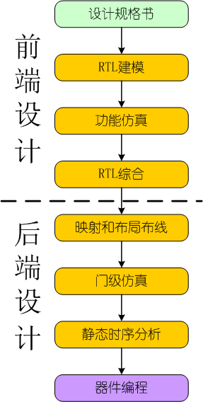
The design process of FPGA is roughly similar to that of ASIC, but there are significant differences in the backend implementation, which also affects how frontend design considerations are approached.
ASIC stands for Application Specific Integrated Circuit, which is a custom integrated circuit designed for specific purposes. Its design process is roughly as follows, and during the specific development process, it involves several development stages, with a more refined division of labor compared to FPGA.
Next, we will summarize some differences between the two from the perspectives of verification and design.
Design Aspects
【Hardware Foundation】
FPGA: It is a pre-manufactured general-purpose programmable chip. It contains a large number of configurable logic blocks, programmable interconnect resources, memory blocks, DSP blocks, clock resources, etc. FPGA design utilizes hardware description language (HDL) to configure these pre-made resources to achieve specific functions.
ASIC: It is a customized chip designed and manufactured from the transistor level based on specific application requirements. ASIC design creates a unique chip that contains only the logic gates, memory, analog circuits, etc., necessary to achieve the target function, with no redundant programmable resources.
【Process and Complexity】
FPGA design process: Relatively simple and quick, mainly consisting of: RTL design -> functional simulation -> synthesis (mapping to the standard cell library/primitive provided by the FPGA vendor) -> place and route (automatically completed by FPGA tools) -> timing analysis -> generate bitstream -> download to FPGA chip. Physical design automation: FPGA vendors have completed the most basic and complex physical design (transistor arrangement and interconnections). Designers only need to focus on logical design, while place and route is handled automatically by tools (though constraints and optimizations are still needed).
ASIC design process: Extremely complex and lengthy, involving complicated design process stages, mainly consisting of: RTL design -> functional simulation -> synthesis (mapping to the standard cell library of the target process) -> physical design -> physical verification (DRC/LVS) -> timing closure (STA) -> power closure -> generate GDSII -> tape-out -> manufacturing (Fab) -> packaging and testing. The physical design challenges are immense: designers (or backend teams) must manually or highly guide tools to complete the physical layout of the chip, clock tree construction (to ensure clock signal quality), power network design, fine routing, etc., while meeting strict timing, power, area, noise, and manufacturability requirements. This is the most time-consuming, complex, and costly phase of ASIC design.
Verification Aspects
【Verification Targets】
FPGA verification: The target of verification is the design implemented on the programmable logic device (FPGA). The FPGA itself is a well-known, reprogrammable chip. The focus of verification is on the functional behavior of the design code after it is mapped to the FPGA device.
Chip verification: The target of verification is the custom chip (ASIC or SoC) that will eventually be manufactured. Verification must ensure the correctness of the RTL functionality of the design and that it meets timing and performance requirements under the target semiconductor process, operating voltage, and temperature range.
【Verification Objectives】
FPGA verification:
Functional correctness: Confirm that the RTL-level functional logic meets expectations.
System integration: Interact with real peripherals (memory, interfaces, sensors, processors, etc.) in an actual hardware environment to verify system-level integration and interface protocols.
Software development and firmware verification: Provide a real hardware platform for embedded software/firmware engineers for development and testing.
Performance evaluation: Assess system performance (throughput, latency) on real hardware, but limited by FPGA architecture and speed grade.
Early market verification/demo: Used for customer demonstrations or early product prototypes.
Chip verification:
Tape-out correctness: The functionality and performance of the chip after tape-out must meet requirements, which is the ultimate goal. Ensure that the design meets all functional, timing, power, reliability, and testability requirements under the target process and PVT conditions. The cost of a tape-out failure is extremely high.
Comprehensive coverage: All possible boundary conditions, extreme timing paths, asynchronous interfaces, low power state transitions, manufacturing defect models, etc., need to be covered. The goal is “zero defects” or as close as possible.
Accurate modeling: It is necessary to accurately simulate the functionality of the chip during RTL simulation, and in post-simulation, accurately verify timing characteristics, simulating physical effects (gate delay, line delay, crosstalk, power noise, temperature effects, etc.).
【Iteration Speed】
FPGA verification: Occurs in the mid to late stages of design, with a very fast iteration speed. After modifying the RTL, it takes only a few minutes to a few hours to synthesize, place and route, generate the bitstream, and download it to the FPGA device for testing. This enables rapid debugging and functional exploration, so FPGA verification is often used for chip prototype verification.
Chip verification: Occurs in the early (functional simulation) and late (timing simulation) stages of chip design, before tape-out. It is an important quality checkpoint before tape-out. The iteration speed is extremely slow. Once tape-out occurs, the manufacturing process takes months, and if major errors are found, the cost is catastrophic. Therefore, it is essential to ensure accuracy through an extremely rigorous verification process before tape-out.
【Verification Methods】
FPGA verification:
Main methods: Hardware in-the-loop testing. Download the design to an FPGA development board or prototype board and connect real peripherals for testing. FPGA simulation tools are commonly used for module-level or small-scale system-level verification. Functional verification is the core.
Timing verification: Relies on static timing analysis reports from FPGA tools and on-board testing. Limited by the fixed architecture of the FPGA (routing resources, clock tree), it cannot accurately simulate the custom clock tree and routing delay distribution of ASIC.
Power verification: Actual power consumption of the FPGA can be measured, but this reflects the power consumption of the FPGA implementation, not the precise power consumption model of the final ASIC.
Physical effects: Generally not considered (determined by FPGA structure).
Coverage: Focus on functional coverage.
Chip verification:
Main methods: Large-scale functional and timing simulation (post-simulation based on gate-level netlist + standard cell library + timing information (SDF)), formal verification, static timing analysis, power analysis (dynamic/static power assessment), physical verification (DRC/LVS), DFT verification (ATPG, scan chain testing). Functionality, timing, and power are all essential.
Gate-level accuracy: Post-simulation is performed on the gate-level netlist, combined with precise timing information (SDF, simulating the actual silicon delay).
Extreme conditions: Verification must be conducted under various PVT corners (fast process corner/slow process corner, high voltage/low voltage, high temperature/low temperature).
Low power verification: Use UPF to verify complex power shutdown, voltage regulation, state retention, and other mechanisms.
Physical effects: Must consider signal integrity (crosstalk, IR Drop), electromigration, and other impacts from physical design.
Coverage: Pursue extremely high functional coverage and code coverage.
Testability: Must verify that DFT structures (scan chains, BIST, boundary scan) are functioning correctly.
Physical Implementation
FPGA physical implementation: It is programming fixed hardware resources. FPGA chips come with a large number of logic blocks (CLB), routing switches, BRAM, DSP, and other fixed physical resources. The physical implementation process is simply mapping the user design to these pre-made resources using EDA tools (like assembling structures on a Lego base). FPGA place and route is highly automated (tools automatically map according to FPGA architecture), and engineers only need to set timing constraints. In clock tree design, FPGA uses vendor-prepared global clock trees, and users can only configure them to a limited extent. In timing closure, it only requires timing closure (STA), with main challenges being: routing congestion leading to timing violations, and fixed DSP/BRAM quantity limiting design scale, etc.
ASIC physical implementation: It is the construction of a chip from scratch, starting from the standard cell library (NAND gates, flip-flops, etc.), precisely placing transistors on a blank silicon wafer, drawing metal interconnections, and constructing clock trees and power networks. It must consider the physical rules of the manufacturing process (such as photolithography accuracy, metal layer stacking). ASIC place and route requires deep manual involvement, needing to plan module locations (floorplanning), optimize critical paths, balance clock skew, etc. In clock tree design, ASIC must synthesize multi-level clock trees from scratch, ensuring low skew and power consumption. In timing closure, it must pass hundreds of DRC (design rule checks), LVS (layout versus schematic consistency), electrical rules (ERC), etc., otherwise, tape-out cannot occur. The main challenges include signal integrity issues, physical effect modeling, etc.
Cost and Risk
【FPGA】
Relatively low cost (mainly FPGA development boards, tool licenses, engineer time). The risk lies in potentially missing some deep issues that only manifest in ASIC implementations or under extreme conditions, but the iteration cost is low. There are no high tape-out costs.
【Chip】
Extremely high cost (verification tools, server resources, a large amount of engineer time, especially the cost of tape-out itself). The risk is extremely high. Insufficient verification leading to tape-out failure can result in huge financial losses and project delays. Therefore, the investment in chip verification (manpower, time, computational resources) is far greater than that of FPGA verification. Tape-out costs (millions to tens of millions of dollars, increasing dramatically with advanced process nodes), mask making costs, testing development costs, etc.
Performance, Power Consumption, and Area
【Performance】
ASIC >> FPGA: ASIC circuits are custom-designed, and the routing is optimized, with no additional delays from programmable interconnections. Clock frequencies can reach GHz levels (especially in advanced processes).
FPGA: Limited by pre-made structures and the delays of programmable switches, it typically operates at frequencies far below those of ASICs in the same process (hundreds of MHz is common, GHz is difficult and has high power consumption).
【Power Consumption】
ASIC << FPGA: ASIC can adopt the most advanced low-power design techniques (clock gating, multi-threshold voltage, power shutdown, near-threshold voltage design, etc.), with transistor-level optimization and very low static power consumption.
FPGA: Relatively high static power consumption (programmable structures consume power even when not in use), and dynamic power consumption is also higher than that of ASICs with similar functionality due to longer interconnections and more switching resources.
【Area/Integration】
ASIC << FPGA: ASIC contains only the logic necessary to implement functionality, with extremely high density, and is much smaller in area than an FPGA that implements the same functionality under the same process.
FPGA: Contains a large number of redundant resources (LUTs, Flip-Flops, Routing Switches) to ensure flexibility, resulting in larger chip area and relatively lower integration.
【Flexibility】
FPGA: Extremely high flexibility, designs can be modified, upgraded, or errors fixed at any time by reprogramming (downloading a new bitstream). Supports field updates.
ASIC: Zero flexibility, once the chip is manufactured, its functionality is fixed and cannot be modified. Any design errors or functional updates require a new tape-out, which is extremely costly.
【Time to Market】
FPGA: Short time to market, short development cycle (weeks to months), no need to wait for a lengthy manufacturing process. Very suitable for rapid prototype verification and products that need to be launched quickly.
ASIC: Long time to market, from design start to final chip mass production, usually takes 1-3 years or even longer (including complex backend design, tape-out, manufacturing, packaging, and testing).
【Risk】
FPGA: Lower risk. Design errors can be quickly and cheaply fixed by reprogramming. There is no risk of tape-out failure.
ASIC: Extremely high risk. Tape-out failure (functional errors, timing violations, power overages, physical design defects, etc.) means tens of millions of dollars in losses and at least 6-12 months of project delays. Verification must be extremely thorough.
Selection
【Choosing FPGA】
Need to quickly prototype and verify designs.
Product requirements may change or require field upgrades/reconfigurations.
Product lifecycle is short or time to market is critical.
Production volume is not large enough to share the high NRE costs of ASIC.
Project budget is limited and cannot bear the risks and costs of ASIC tape-out.
System requires high parallel processing and does not have extremely stringent performance/power requirements.
【Choosing ASIC】
Pursuing performance (speed), power consumption, area/cost (in large volumes).
Product definition is very stable and has a long lifecycle.
Expected production volume is very large (usually millions or more), enough to amortize the huge NRE costs.
Have sufficient funds, time, and technical capabilities to handle complex design processes and high risks.
Target market has extreme requirements for size and power consumption (such as mobile SoCs, wearable devices, high-performance computing chips).
In summary, FPGA is like quickly building a “house” (function) with ready-made “Lego blocks” (pre-made resources), flexible but not as refined and efficient; ASIC is like hiring architects and workers to build a “skyscraper” (chip) from scratch (transistors) according to your blueprint, which cannot be changed once built, but offers superior performance, efficiency, and cost in large volumes compared to a Lego house.
Both have their pros and cons, and the choice depends on specific application scenarios, budget, time, risk tolerance, and performance requirements. In modern complex system design, FPGAs are often used for ASIC prototype verification and early development.
Recommended Reading


Click to read the original text for IC design job consultation