Since the emergence of ChatGPT at the end of 2022, followed by the hundred-model battle in 2023, and the recent releases of GPT-4.5 by OpenAI, Grok3 by xAI, Claude 3.7 Sonnet by Anthropic, and Llama4 by Meta, the iteration speed of large models has been accelerating. In China, there has been a surge in open-source developments, with DeepSeek releasing V3 and R1, and Alibaba’s Tongyi Qianwen launching a new inference model QwQ-32B. Under such developments, the number of generative AI users in China has reached 300 million, exceeding 20% of the population, up from 249 million at the end of last year, marking an increase of over 50 million in just three months.
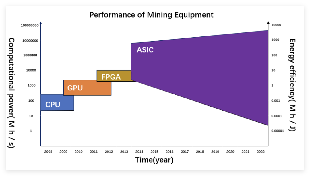
For AI large models, deployment is the most urgent task. Therefore, the second half of the AI chip battle has gradually shifted from the training end to the inference end. From the perspective of device form, ASICs are certainly more efficient for AI inference.
Yesterday, Google’s most powerful AI chip, the seventh-generation TPU (Tensor Processing Unit) – Ironwood, was officially unveiled. This TPU chip boasts a performance increase of 3600 times, directly challenging NVIDIA’s Blackwell B200. This may indicate that the war for ASICs has advanced further.
ASIC: Complementing GPUs
As is well known,ASICs are custom chips whose computing power and efficiency are strictly matched to task algorithms. The number of chip cores, the ratio of logic computing units, control units, cache, and chip architecture are all precisely customized, thusASICs possess valuable performance, size, and power consumption characteristics.
However, in contrast, the development of ASICs requires a long development cycle and carries significant development risks, which is why NVIDIA’s GPUs have triumphed in the AI era with their powerful general-purpose computing power and software ecosystem.
Manufacturers’ pursuit of energy efficiency and cost is relentless. Major cloud computing and large model companies such as Google, Amazon, Meta, and OpenAI are accelerating their layout of customized ASICs, which are gradually becoming an important new technological route alongside NVIDIA’s GPUs. Morgan Stanley predicts that the AI ASIC market size will grow from $12 billion in 2024 to $30 billion in 2027, with a compound annual growth rate of 34%.
For AI training, strong parallel computing power is required, while the demand for computing power in AI inference is lower, and the algorithms are relatively fixed. Additionally, many companies have completed the R&D of their ASICs. Therefore, a situation is gradually forming where NVIDIA’s GPUs dominate AI training, while more manufacturers are turning to ASIC chips for inference. Of course, there are exceptions, such as Apple choosing to use Google’s TPU for model training.
The emergence of DeepSeek has further pushed the industry to focus on inference limits, enhancing computing efficiency and reducing costs, making the competitive landscape more diverse. It is important to emphasize that ASICs will not replace GPUs but will collaborate with them.
Google TPU: Performance Takes Off Again
TPUs are ASIC chips specifically designed for processing tensor operations, with the first product launched by Google in 2016. In the world of deep learning, tensors (multi-dimensional arrays) are ubiquitous. TPUs were born to efficiently handle these tensor operations.
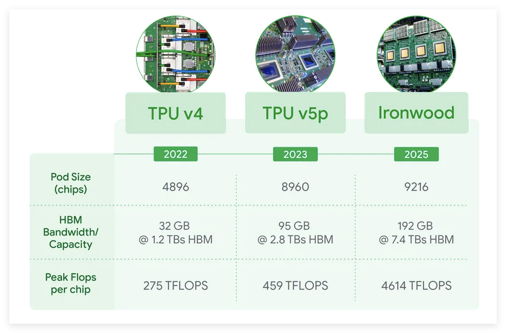
Yesterday, Google officially released its seventh-generation Tensor Processing Unit (TPU) Ironwood. Google claims that under large-scale deployment, this AI accelerator’s computing power can exceed that of the world’s fastest supercomputer by more than 24 times.
In terms of single-chip specifications, Ironwood significantly enhances memory and bandwidth, with each chip equipped with 192GB of high-bandwidth memory (HBM), six times that of the previous generation TPU Trillium released last year. Each chip’s memory bandwidth reaches 7.2 terabits/s, which is 4.5 times that of Trillium.
Additionally, Ironwood boasts super specifications, providing 42.5 exaflops of AI computing power when each pod expands to 9216 chips, far exceeding the 1.7 exaflops of the current fastest supercomputer, El Capitan. Each Ironwood chip has a peak computing capability of 4614 TFLOPs.
Currently, TPU chips have become the third-largest data center chip design manufacturer globally. According to industry insiders, the production volume of Google’s TPU chips last year reached between 2.8 million and 3 million units.
Domestic TPU: A Fully Self-Developed Product Taking 5 Years
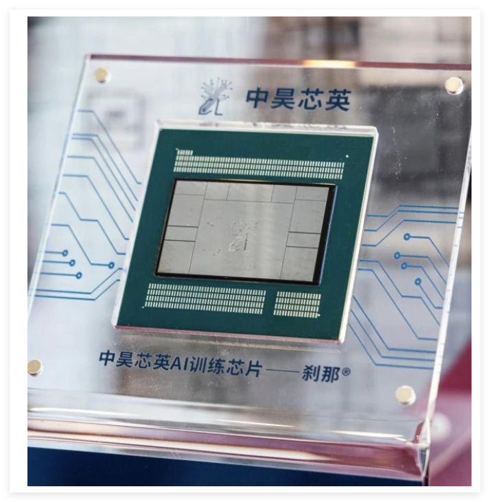
There is also a domestic manufacturer laying out TPUs, which is Zhonghao Xinying.
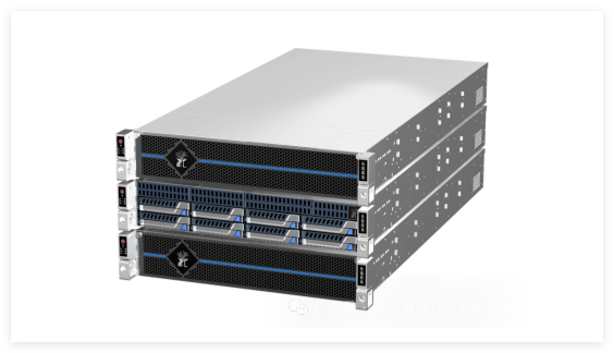
Zhonghao Xinying was founded in 2018 by Yang Gongyifan, a core developer of Google’s TPU chip, along with a team of AI hardware and software design experts from overseas tech giants such as Google, Microsoft, and Samsung. The company aims to build a high-performance AI chip “Shanai” based on its self-developed TPU architecture and the computing cluster “Taize®”, which is controllable and can match overseas advanced levels, serving as the cornerstone for AI large model computing. It has currently collaborated with various local governments, operators, and enterprises to build multiple ultra-large-scale intelligent computing centers.
Founder Yang Gongyifan holds a master’s degree from Stanford University and a bachelor’s degree from the University of Michigan, with 54 Chinese patents and 15 patents in the US and Europe. He has published three top papers in ASSCC/ISSCC/JSSCC and has over ten years of experience in high-end chip R&D in Silicon Valley, having led the development of Google TPU 2/3/4 chips and designed 12 high-performance CPUs, including Oracle’s SPARC T8/M8, with over ten successful tape-outs.
In terms of products, China’s first high-performance TPU architecture AI chip “Shanai” is a high-performance AI chip based on the GPTPU architecture, fully self-developed over nearly five years, with completely controllable IP cores, self-developed instruction sets, and computing platforms. In AI large model computing scenarios, “Shanai”‘s computing performance surpasses that of well-known overseas GPU products by nearly 1.5 times, with a 30% reduction in energy consumption, successfully breaking the monopoly of foreign enterprises in the high-end AI chip field.
“Shanai” achieves reconfigurable multi-level storage, a compute-storage integrated design, and a pipeline-style spatiotemporal mapping, enhancing both the speed and accuracy of large model computing with powerful parallel processing capabilities. It also employs Chiplet technology, achieving performance leaps under the same process technology through 2.5D packaging. It supports interconnection between 1024 chips, with system cluster performance far exceeding traditional GPUs by dozens of times, and performance can grow linearly during cluster expansion, enabling the construction of supercomputing clusters with thousands or tens of thousands of cards.
The “Taize” AI computing cluster system built on the “Shanai” chip achieves high-speed interconnection between 1024 AI chips, allowing for linear scalability, with a maximum floating-point computing capability of over 200P per cluster. The system-level performance is dozens of times higher than traditional GPU clusters, and the “Taize®” large-scale AI computing cluster can support various high-intensity AI computing scenarios, including ultra-large parameter AIGC large model computations, advanced autonomous driving model training, precise protein structure prediction, AlphaGo, AlphaZero, and more.
LPU: Groq Takes Off
In the era of AI large models,LPU has emerged as a new type of ASIC that is being wildly praised.
As early as January this year, it was reported that the US inference chip company Groq had successfully run DeepSeek on its LPU chip, achieving efficiency an order of magnitude faster than the latest H100, reaching 24000 tokens per second.
Additionally, Groq built the largest inference cluster in the Middle East, including 19000 Groq LPUs, in Dammam, Saudi Arabia in December 2024.
So what exactly is an LPU?
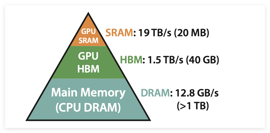
Essentially, an LPU is a new type of hardware processor (ASIC chip) specifically designed for processing natural language (NLP) tasks. However, what sets LPU apart from other ASICs is its storage. It adopts a compute-storage integrated design, replacing the HBM in GPUs with lower-capacity but faster SRAM. By directly integrating high-bandwidth on-chip SRAM into the chip, it effectively reduces memory access latency and significantly enhances overall computational throughput. In simple terms, it is ASIC + compute-storage integration, making it faster than GPUs.
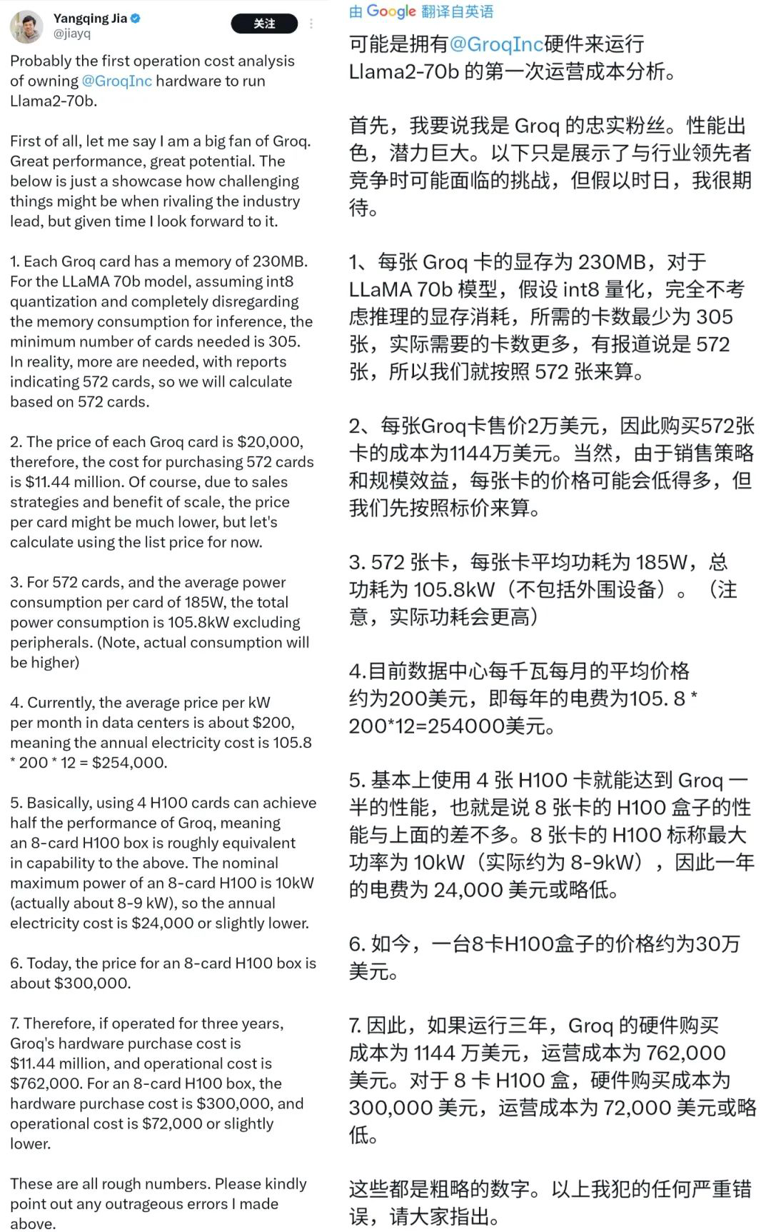
However, while switching to SRAM does indeed speed things up, the overall cost may actually be higher. It has been roughly calculated that over a three-year operational cost, the procurement cost of Groq LPU would be 38 times that of NVIDIA’s H100, with operational costs reaching ten times. From this perspective, the LPU may not be as “mythical” or “game-changing” as the media portrays.
While LPU may not match GPUs in terms of versatility and cost-effectiveness, it has indeed significantly improved computing power and has a good energy efficiency ratio, making it a viable route.
NPU: The New Darling of the Era
Unlike TPUs and LPUs, NPUs are primarily used in edge AI. As large models inject new vitality into AI, the demand for edge AI has also increased. Major processor IP manufacturers are expanding their edge-based AI NPU offerings to offload CPU loads, thereby improving efficiency and reducing power consumption. Some MCU manufacturers have integrated NPU cores into their products, including NXP, TI, Infineon, ST, and ADI, all using self-developed NPU IP cores. There are also some third-party NPU IP manufacturers in the market:
Arm Ethos NPU: Launched the Ethos-U55 in early 2020, now in its third generation, including Ethos-U55 and Ethos-U65. Products based on the Cortex-M55 + Ethos-U55 combination have been launched by ALIF, Himax, Nuvoton, and Infineon.
Andes Technology: In 2023, Andes released its self-developed “Zhouyi” X2 NPU, optimized for various applications such as ADAS, smart cockpits, tablets, desktops, and smartphones. Additionally, Andes has the “Zhouyi” Z series NPUs. Notably, Andes’ new generation “Zhouyi” NPU achieves efficient deployment of DeepSeek-R1 on the edge.
Ceva: Specific products include Ceva-NeuPro-Nano, Ceva-NeuPro-M, and Ceva-NeuPro Studio.
Cadence: Cadence’s Tensilica Neo NPU is a high-performance, low-power neural processing unit (NPU) designed for embedded AI applications.
Synopsys: The Synopsys ARC NPX6 NPU IP series is the industry’s highest-performing neural processing unit (NPU) IP, designed to meet the real-time computing needs of AI applications with ultra-low power consumption. This series includes ARC NPX6 and NPX6FS, supporting the latest complex neural network models, including generative AI, and providing up to 3500 TOPS of performance, suitable for smart SoC designs.
Chipone: Officially stated that its NPU IP AI chips have shipped over 100 million units globally, mainly applied in IoT, wearables, smart homes, security monitoring, servers, automotive electronics, smartphones, and tablets. Its NPU IP has been used by 72 customers in 128 AI chips. The latest VIP9000 series NPU IP offers scalable and high-performance processing capabilities, suitable for Transformer and convolutional neural networks (CNN).
Andes Technology: The AndesAIRE AnDLA I350 is a deep learning accelerator designed for edge and terminal inference, providing high performance and efficient AI solutions.
Other ASIC Chips: Waiting for Opportunities
In the ASIC field, Broadcom and Marvell are two major players, holding about 70% of the market share in AI custom chips.
Broadcom’s core advantage in AI chips lies in customized ASIC chips and high-speed data exchange chips, with solutions widely used in data centers, cloud computing, HPC (high-performance computing), and 5G infrastructure. The latest financial report shows that Broadcom’s AI-related business revenue surged by 220% year-on-year, mainly driven by strong demand for AI accelerators and networking equipment. Broadcom CEO Hock Tan revealed in the earnings call that by 2027, the demand for AI custom chips from its three major clients is expected to reach $60 billion to $90 billion.
Broadcom has two major collaborations that are attracting attention: the first is with Meta, which has developed the first two generations of AI training acceleration processors, and both parties are accelerating the development of the third-generation MTIA chip, expected to make significant progress in the second half of 2024 to 2025. The second is that OpenAI has commissioned Broadcom to develop two generations of ASIC chip projects, planned for production in 2026, which will adopt industry-leading 3nm/2nm process technology along with advanced 3D SOIC packaging technology. Meanwhile, although Apple is still using Google’s TPU, its self-developed AI chip project is actively progressing.
Marvell’s custom ASIC business is becoming a key engine for its growth. In 2019, Marvell acquired Avera Semiconductor from GlobalFoundries for $740 million, officially entering the ASIC market. This business has successfully attracted orders from tech giants like Amazon and Google.
In December 2024, Marvell reached a five-year multi-generation cooperation agreement with AWS (Amazon Web Services) covering AI chip custom design, further deepening its layout in the cloud computing market. Marvell predicts that as the demand for AI computing power explodes, the proportion of its ASIC business will increase to 25%, and it expects the data center ASIC market size to grow to $42.9 billion by 2028.
At the end of last year, AWS released its next-generation AI training chip Trainium3. This is the first AWS chip manufactured using a 3nm process node, achieving a 40% increase in energy efficiency and doubling performance. The UltraServer equipped with Trainium3 is expected to outperform the Trn2 UltraServer by four times. The first instances based on Trainium3 are expected to be launched by the end of 2025.
In 2023, Microsoft also released its AI chip (ASIC) Microsoft Azure Maia 100, specifically designed for cloud training and inference. Maia 100 is Microsoft’s first AI chip designed for training and inference of large language models in Microsoft Cloud, using TSMC’s 5nm process, with a transistor count of 105 billion, making it not lightweight when it comes to transistors or clock speed. It is also optimized for AI and generative AI, supporting Microsoft’s first implementation of data types below 8 bits (MX data types).
Conclusion
ASICs will not completely replace GPUs but will become the dominant force in the inference market and will also develop in the training field. Innovations such as Google’s TPU, domestic “Shanai”, and Groq LPU are driving AI computing power towards efficiency and low cost. In the future, as large models continue to evolve, ASICs will undoubtedly see further development.
References
[1] China Electronics News: https://mp.weixin.qq.com/s/1Drsaz4gfkLQC3TjvaoV6w
[2] Fresh Date Classroom: https://mp.weixin.qq.com/s/9i5qcCGZj1ynCkTfsA01Yg
[3] Machine Heart: https://mp.weixin.qq.com/s/MQRWr_i76Vrw8Z5YQaIbeA
[4] Tencent Research Institute: https://mp.weixin.qq.com/s/-KhpFHznaLlvbkkIUlSW_A
[5] Negative Review: https://mp.weixin.qq.com/s/I4ox6Ir5xk3MvwKbVH3grQ
· END ·
Follow the subscription account under EEWorld: "Robot Development Circle"
Reply "DS" to receive the complete version of "DeepSeek: From Beginner to Master"

Scan to add the assistant and reply “robot”
Join the group to exchange experiences face-to-face with electronic engineers