SoC Design Organizational Structure
-
1. SoC Architecture Design Department
-
SoC Architect/Manager: Leads the chip system architecture design (including computation/storage/bus architecture, low-power strategies), responsible for competitive analysis and technical roadmap formulation..
-
System Design Engineer: Translates architecture into microarchitecture design, defines module interfaces and PPA targets..
2. Front-end Design Department
-
IP Integration Engineer: Responsible for bus design (AXI/APB, etc.), IP selection and integration..
-
RTL Design Engineer: Completes module-level RTL coding, timing optimization, and low-power design..
3. Verification and Back-end Department
-
Verification Team: Builds UVM platform, responsible for functional/power verification and coverage convergence..
-
Back-end Team: Responsible for physical design, timing closure, and DFT testing..
4. Cross-functional Support Department
Firmware Team: Develops chip drivers and operating systems, participates in hardware-software co-verification.
-
Application Team: Provides customer support and overall solutions.
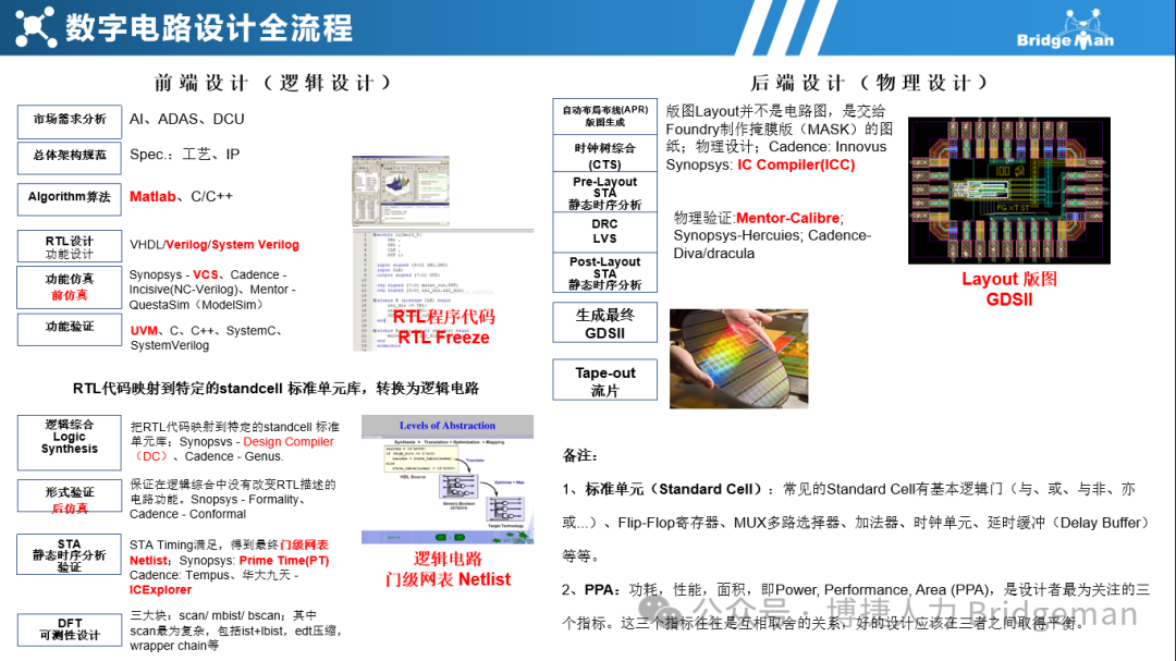
Key Collaborative Positions and Interaction Processes
The core collaborative relationships of SoC system design engineers are as follows (with overlapping responsibilities):
| Collaborative Position | Collaboration Content | Key Outputs |
|---|---|---|
| Verification Engineer | Jointly formulate verification plans, provide test cases, and locate design defects. | Verification report/coverage analysis |
| Back-end Engineer | Provides timing constraints (SDC/UPF), collaborates to optimize PPA. | Timing closure report/power analysis |
| Firmware Engineer | Defines hardware register mapping, supports driver development and chip startup debugging. | Hardware-software interface documentation |
| Algorithm Engineer | Transforms high-frequency algorithms into hardware acceleration modules (e.g., NPU/codec). | Hardware acceleration solution documentation |
| Product Manager | Undertakes market demands, clarifies chip specification definitions. | Product Requirement Document (PRD) |
Core Job Responsibilities
1. System Architecture Definition
Participates in chip specification (Spec) formulation, completes hardware-software partitioning, computing power allocation, and bus bandwidth/latency analysis.
Leads IP selection evaluation (e.g., CPU/GPU/NPU, etc.) and subsystem data flow design.
-
2. Front-end Design and Integration
RTL coding, clock/reset/low-power scheme design (UPF/SDC constraints).
NoC bus integration, IP interface module development (AXI/CHI protocols, etc.).
-
3. Cross-team Collaboration
Jointly develop test plans with the verification team, locate design defects, and ensure coverage convergence.
Provides netlist and timing constraints to the back-end team, collaborates to optimize PPA (Performance/Power/Area).
Supports the firmware team in completing register mapping and driver debugging.
-
4. Tape-out Support and Optimization
Participates in FPGA prototype verification, chip back-testing, and mass production issue troubleshooting.
System-level performance analysis (Profiling) and optimization (e.g., resolving DDR bandwidth bottlenecks).
Job Requirements
| Category | Specific Requirements |
|---|---|
| Education and Major | Bachelor’s degree or above in Microelectronics/Computer/Electronics, master’s degree generally required for large companies and high-end positions. |
| Tool Skills | Proficient in using Verilog/SystemVerilog, Python/Tcl scripts, DC/PT/Spyglass and other EDA tools. |
| Protocol Mastery | Must be proficient in AMBA bus (AXI/APB/AHB), low-power design processes (UPF). |
| Experience | Junior positions: 1-3 years, Senior positions: 3-5 years, Architect positions require 8+ years of tape-out experience. |
Differentiated Competitive Advantages
IP Integration Experience: Automotive-grade chips (CAN/Ethernet), AI accelerators (NPU/DSP), high-speed interfaces (PCIe/DDR5).
Vertical Domain Expertise: Functional safety (ISO 26262), secure encryption modules (AES/RSA).
Full Process Capability: Experience participating in the entire cycle from architecture definition to mass production support.
Transformation Strategies for Non-SoC Background Talent
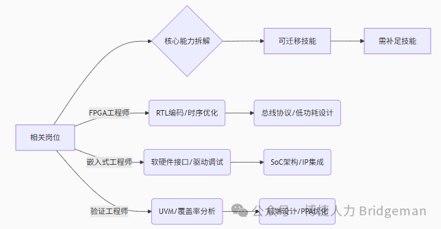
For candidates from non-SoC design positions (such as FPGA engineers, embedded developers, verification engineers), a stepwise capability transition path needs to be designed:
1. Capability Migration Path
2. Transformation Training Program
-
Knowledge Supplement:
Required Courses: In-depth study of AMBA bus protocol, practical low-power design with UPF, NoC architecture design.
Project Practice: Complete the full process of IP integration through open-source SoC projects (e.g., RISC-V Mini).
-
Experience Focus:
-
Highlight “cross-position collaboration achievements” in resumes (e.g., “Collaborated with design team to optimize DDR timing, improving bandwidth utilization”).
Transform algorithm/driver development experience into “hardware acceleration solution design capability”.
Salary and Recruitment Trends (Latest Data for 2025)
| Job Level | Annual Salary Range (10,000 RMB) | Hot Demand Areas |
|---|---|---|
| Junior Engineer (1-3 years) | 250,000-400,000 | Consumer Electronics/IP Integration |
| Senior Engineer (3-8 years) | 450,000-750,000 | Automotive-grade Chips/AI Accelerators |
| Architect (8+ years) | 800,000-1,500,000+ | Chiplet/Unified Memory and Computing |
💡 Practical Tips:
Successful Case of Cross-Position Transformation: An embedded engineer successfully transitioned to lead the design of an intelligent cockpit SoC by leveraging Linux driver experience and supplementing AXI protocol knowledge.;
Risk Avoidance Points: Transitioning from verification to design requires caution against “fixed mindset” (overly focusing on test cases rather than architectural rationality).;
Recommended Toolkits: Open-source SoC learning platforms, AMBA protocol quick reference manual.
