
SPI (Serial Peripheral Interface) is a synchronous serial communication protocol used for data transmission between devices over short distances. It is commonly used for communication between microcontrollers and external devices such as sensors, flash memory, displays, etc. SPI has the following main characteristics:
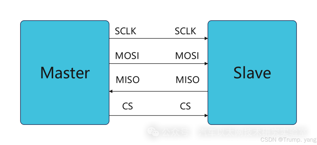
SPI is a master-slave communication protocol, typically consisting of one master device and one or more slave devices. The master device controls the timing of the communication, and the slave devices respond according to the instructions from the master device.
SPI uses the following four main signal lines:
-
MOSI (Master Out Slave In): The line for the master device to send data to the slave device.
-
MISO (Master In Slave Out): The line for the slave device to send data to the master device.
-
SCLK (Serial Clock): The clock signal generated by the master device, used to synchronize data transmission.
-
CS (Chip Select): Used to select a specific slave device for communication, typically activated by a low level.
SPI forms 4 operating modes (Mode 0, 1, 2, 3) through different combinations of clock signal phases and polarities. These 4 modes determine the timing of data sampling and transmission based on the polarity (CPOL) and phase (CPHA) of SCLK.
-
Full-Duplex Synchronous Communication: SPI allows simultaneous data sending and receiving, enabling both the master and slave devices to send and receive data at the same time.
-
High Speed: Due to hardware-controlled synchronous communication, SPI has a higher transmission speed, typically faster than other protocols like I²C.
-
Multiple Slave Devices: A single master device can control multiple slave devices by selecting different slave devices through individual CS lines.
-
Simple Protocol: The SPI protocol does not have complex arbitration or addressing mechanisms, making it relatively easy to implement.
In SPI communication, the addressing method is mainly implemented through the chip select (Chip Select, CS) line. Unlike protocols like I²C, SPI does not have a built-in addressing mechanism, and the selection and management of slave devices are done as follows:
SPI uses the chip select line (also known as the slave select line, SS/CS) to select which slave device to communicate with. The master device needs to send an enable signal to the corresponding slave device’s CS line. Each slave device typically has its own dedicated CS pin. When the master device needs to communicate with a specific slave device, it will pull the corresponding CS line low (i.e., set it to low level, active low; high level can also be used depending on the slave), indicating the selection of that slave device for communication. Other unselected slave devices keep their CS lines high and do not participate in communication.
2. Multiple Slave Device Communication
If there are multiple slave devices on a single SPI bus, the master device needs to provide a separate CS line for each slave device. A typical SPI multiple slave device communication process is as follows:
-
The master device selects the slave device by pulling down the CS line of that slave device.
-
The CS lines of other unselected slave devices remain high, so they do not respond to SPI communication signals.
-
The selected device receives data through the MOSI line and sends data to the master device through the MISO line.
-
When the communication ends, the master device pulls the CS line of that slave device high, stopping communication with that device.
For example, if there are 3 slave devices, the master device may need 3 CS lines to control each slave device, labeled as CS1, CS2, CS3. When the master device wants to communicate with slave device 2, it will pull down CS2 for communication while keeping CS1 and CS3 high.
In some special scenarios, multiple slave devices can be connected in a daisy chain on a single SPI bus. In daisy-chain mode, the slave devices are connected sequentially, and data flows from one slave device to the next. This mode can save pin count on the master device by reducing the number of CS lines, but the communication method is more complex.
In daisy-chain mode, the master device sends data through the serial clock (SCLK), and the data passes through each slave device sequentially. After the data has passed through all slave devices, the last slave device returns the data to the master device. This mode is typically used for certain types of devices, such as LED drivers or shift registers.
4. Address Registers (Application Layer)
Although the SPI protocol itself does not have a device addressing mechanism, similar addressing functionality can be implemented through application layer protocols. The first byte or the first few bits sent by the master device can be defined as the virtual address of the device, and only the slave device that matches this address will respond. In this way, the SPI addressing logic needs to be designed and implemented through hardware or software protocols.
SPI Communication Process
Clock Signal Generation (SCLK)
The clock signal (SCLK) generated by the master device is used to synchronize data transmission. Data is sampled or sent on the rising or falling edge of the clock (depending on the configured CPOL and CPHA mode).
Data Transmission (MOSI/MISO)
-
Data Sending (MOSI): The master device sends data to the slave device through the MOSI (Master Out Slave In) line. The master and slave devices synchronize data transmission according to the protocol settings on the corresponding clock edge.
-
Data Receiving (MISO): Simultaneously, the slave device can send data to the master device through the MISO (Master In Slave Out) line. Since SPI is full-duplex communication, data sending and receiving can occur simultaneously.
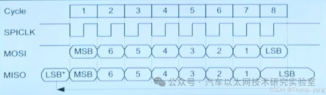
Typically, the data bit count is 8 bits, and the master device does not require the slave device to acknowledge after sending a byte. After sending one data byte, it immediately sends the next byte. The order of data transmission is generally from the most significant bit (MSB) to the least significant bit (LSB), but it can also be changed through configuration.
Data Sampling and Shifting
-
During data transmission, data bits are sent out on one edge of the clock and received on another edge. The specific data sampling timing depends on the clock polarity (CPOL) and phase (CPHA).
-
The master and slave devices have shift registers inside, and each clock pulse causes the data in the shift register to shift left one bit until the entire byte is sent and received.
Communication Timing Diagram
In SPI communication, clock polarity (CPOL) and phase (CPHA) are two important parameters used to define the characteristics of the clock signal and the timing of data sampling. These two parameters determine when data is sent and received. To ensure correct communication between the master and slave devices, both parties must have consistent clock polarity and phase.
CPOL defines the level of the clock signal in the idle state.
-
CPOL = 0: The clock line is low in the idle state.
-
CPOL = 1: The clock line is high in the idle state.
CPHA defines the timing of data sampling, i.e., on which edge of the clock data is sampled.
-
CPHA = 0: Data is sampled or sent on the first clock edge (the first transition edge of the clock pulse, such as the rising or falling edge).
-
CPHA = 1: Data is sampled or sent on the second clock edge (the second transition edge of the clock pulse, such as the rising or falling edge).
Based on the combinations of CPOL and CPHA, SPI has 4 operating modes. These modes specify the characteristics of the clock signal and the timing of data transmission. Both the master and slave devices must operate in the same mode to ensure correct communication.
Mode 0: CPOL = 0, CPHA = 0
-
The clock idle state is low.
-
Data is sampled on the rising edge (the first edge) and sent on the falling edge.
-
The clock is low, and data is sampled on the first rising edge.
Mode 1: CPOL = 0, CPHA = 1
-
The clock idle state is low.
-
Data is sampled on the falling edge (the second edge) and sent on the rising edge.
-
The clock is low, with data sent on the first rising edge and sampled on the second falling edge.
Mode 2: CPOL = 1, CPHA = 0
-
The clock idle state is high.
-
Data is sampled on the falling edge (the first edge) and sent on the rising edge.
-
The clock is high, with data sampled on the first falling edge.
Mode 3: CPOL = 1, CPHA = 1
-
The clock idle state is high.
-
Data is sampled on the rising edge (the second edge) and sent on the falling edge.
-
The clock is high, with data sent on the first falling edge and sampled on the second rising edge.
How to Choose CPOL and CPHA
-
CPOL determines the idle state of the clock (high or low).
-
CPHA determines whether data is sampled on the first edge (rising or falling) or the second edge.
-
Different devices may require different operating modes, so when selecting CPOL and CPHA, refer to the specifications of the slave devices. The SPI modes of the master and slave devices must match for successful communication.


*Disclaimer: This article is either original or forwarded by the author. If it inadvertently infringes on someone’s intellectual property rights, please inform us for deletion. The above images and text are sourced from the internet; if there are any infringements, please contact us promptly, and we will delete them within 24 hours. The content of the article reflects the author’s personal views, and the Automotive Ethernet Technology Research Laboratory reprints it solely to convey a different perspective, which does not represent the Automotive Ethernet Technology Research Laboratory’s endorsement or support for this view. If there are any objections, please feel free to contact the Automotive Ethernet Technology Research Laboratory.
https://blog.csdn.net/weixin_46999174/article/details/142300663