Hello everyone! Through our previous lessons, we have gained an understanding of how to use the ICD2 emulator and enhanced PIC development board. We have learned how to control resources such as LEDs, relays, buzzers, buttons, seven-segment displays, RS232 serial, stepper motors, and temperature sensors with microcontrollers. You must have felt the ease of use and learnability of the development board. After successfully experimenting with the previous examples, you must be excited and feel a sense of achievement!Now, let’s take the next step and learn about the working principle and usage of the I2C bus. This way, we can store some data we want to keep in the non-volatile memory of the I2C bus, achieving power-off retention. For example:If you set a password, you don’t want to reset it every time the device loses power. We can write the password data into the non-volatile memory. Also, the readings of a car’s odometer are continuously accumulated, which can be achieved by continuously accessing the I2C memory.
1. Features of the I2C Bus
The I2C bus is a master-slave structure where the microcontroller is the master device, and the memory is the slave device. A single bus can support multiple slave devices (it can also have a multi-master structure). The SDA and SCL lines of the I2C bus are bidirectional and use an open-drain structure, connected to the positive power supply through pull-up resistors.During data transmission, the data on the SDA line must remain stable during the high level period of the clock. The high or low state of the data line can only change when the SCL line’s clock signal is low, as shown in Figure 1.
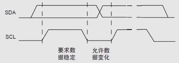
Figure 1: Validity of Data Bits
When the SCL line is high, switching the SDA line from high to low indicates a start condition; when SCL is high, switching the SDA line from low to high indicates a stop condition, as shown in Figure 2.
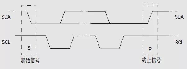
Figure 2: Start and Stop Signals
Each byte sent on the SDA line must be 8 bits. Multiple bytes can be transmitted from high bit to low bit. Each byte must be followed by an acknowledgment bit (ACK). The acknowledgment clock pulse is generated by the master. The master releases the SDA line, and the slave pulls the SDA line low, maintaining stability during the high level of the clock pulse, as shown in Figure 3. When the master receives data, it must send a signal to the slave to terminate the transmission after receiving the last data byte. This signal is achieved by the master sending a “no-acknowledge” to the slave. The slave then releases the SDA line to allow the master to send a stop or repeated start signal.
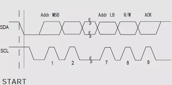
Figure 3: Byte Format and Acknowledgment
2. Data Frame Format
(1) The master sends data to the slave, and the direction of data transfer does not change during transmission, as shown in Figure 4.
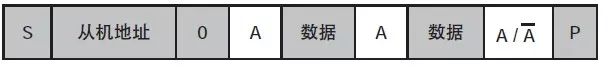
Figure 4: Master Sending Data to Slave
Note: The shaded part indicates data sent from the master to the slave; the unshaded part indicates data read by the master from the slave.
A: indicates acknowledgment;  indicates no acknowledgment.S: Start signal; P: Stop signal.
(2) The master immediately reads data from the slave after the first byte, as shown in Figure 5.
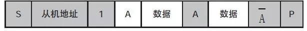
Figure 5: Master Immediately Reads from Slave After First Byte
(3) Composite format, as shown in Figure 6. When the transmission direction changes, the start condition and slave address are repeated, but the R/W bit is inverted. If the master receiver sends a stop or repeated start signal, it should have previously sent a no-acknowledge signal.

Figure 6: Composite Format
From the above formats, it can be seen that regardless of the transmission method, the start signal, stop signal, and address are all sent by the master (the shaded part in the figure), while the direction of data byte transmission is determined by the direction bit in the addressing byte. Each byte transfer must have an acknowledgment bit (A or no acknowledgment).
Next, we will program the 24C02 on the enhanced PIC development board, with the hardware schematic shown in Figure 7. U7 represents the 24C02 chip on the development board, with SDA connected to the microcontroller’s RB5 pin and SCL connected to the microcontroller’s RB4 pin. The seven-segment displays D5, D7, and D8 form the display unit, with font code data input through the RC pin, and the display chip select signals controlled by different RA pins.
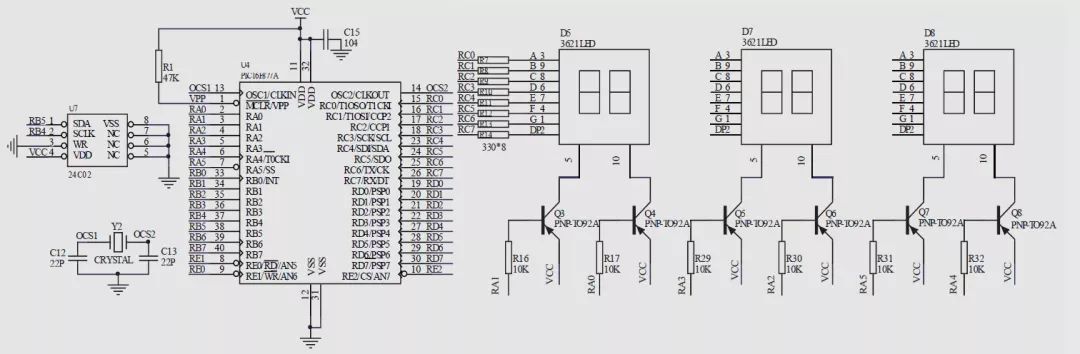
Figure 7: Schematic of Reading/Writing AT24C Series Memory
In the MPLab IDE software, create a new project, add the source code, and configure the chip model and configuration bits. The chip model we use for the experiment is PIC16F877A.
The program code written is as follows, with the program flowchart shown in Figure 8.
3. Software Flowchart
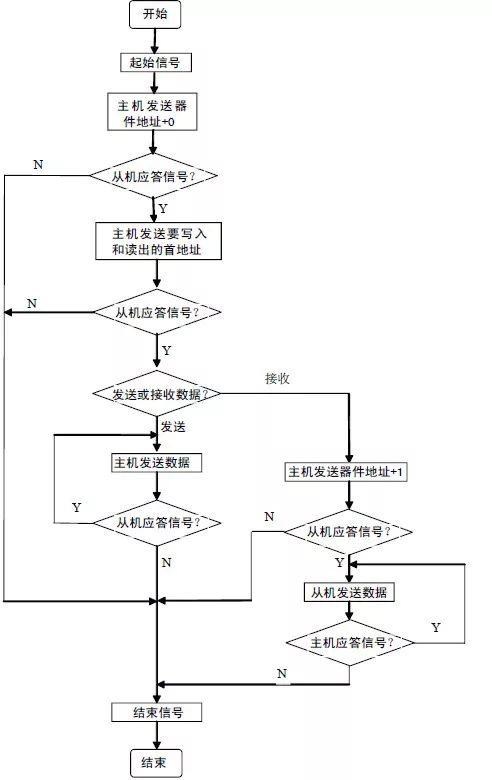
Figure 8: I2C Bus Read/Write Data Flowchart
4. Software Code
/**********/
/* Target Device: PIC16F877A */
/* Crystal Frequency: 4.0MHZ */
/* Compilation Environment: MPLAB V7.51 */
/**********/
/**********
Include Header Files
**********/
#include<pic.h>
/**********
Data Definitions
**********/
#define address 0xa
#define nop() asm(“nop”)
#define OP_READ 0xa1
// Device address and read operation
#define OP_WRITE 0xa0
// Device address and write operation
/**********
Port Definitions
**********/
#define SCL RB4
#define SDA RB5
#define SCLIO TRISB4
#define SDAIO TRISB5
/**********
Common Cathode LED Segment Code Table
**********/
const char table[]={0xC0,0xF9,0xA4,0xB0,0x99,0x92,0x82,0xF8,0x80,0x90,0x88,0x83,0xC6,0xA1,0x86,0x8E};
/**********
Function: Delay Subroutine
**********/
void delay() {
int i;
for(i=0;i<100;i++) {;}
}
/**********
Function: Start Signal
**********/
void start() {
SDA=1;
nop();
SCL=1;
nop();nop();nop();nop();nop();
SDA=0;
nop();nop();nop();nop();nop();
SCL=0;
nop();nop();
}
/**********
Function: Stop Signal
**********/
void stop() {
SDA=0;
nop();
SCL=1;
nop();nop();nop();nop();nop();
SDA=1;
nop();nop();nop();nop();
}
/**********
Function: Read Data
Output Parameter: read_data
**********/
unsigned char shin() {
unsigned char i,read_data;
for(i=0;i<8;i++) { nop();nop();nop();
SCL=1;
nop();nop();
read_data《=1;
if(SDA == 1) read_data=read_data+1;
nop();
SCL=0;
}
return(read_data);
}
/**********
Function: Write Data to EEPROM
Input Parameter: write_data
Output Parameter: ack_bit
**********/
bit shout(unsigned char write_data) {
unsigned char i;
unsigned char ack_bit;
for(i = 0; i < 8; i++) {
if(write_data&0x80) SDA=1;
else SDA=0;
nop();
SCL = 1;
nop();nop();nop();nop();nop();
SCL = 0;
nop();
write_data《= 1;
}
nop();nop();
SDA = 1;
nop();nop();
SCL = 1;
nop();nop();nop();
ack_bit = SDA; // Read Acknowledgment
SCL = 0;
nop();nop();
return ack_bit;
// Return AT24Cxx Acknowledgment Bit
}
/**********
Function: Write Data to Specified Address
Input Parameters: addr, write_data
**********/
void write_byte(unsigned char addr, unsigned char write_data) {
start();
shout(OP_WRITE);
shout(addr);
SDAIO = 0;
// Set SDA as output before writing data
shout(write_data);
stop();
delay();
}
/**********
Function: Read Data from Specified Address
Input Parameter: random_addr
Output Parameter: read_data
**********/
unsigned char read_random(unsigned char random_addr) { unsigned char read_data;
start();
shout(OP_WRITE);
shout(random_addr);
start();
shout(OP_READ);
SDAIO = 1;
// Set SDA as input before reading data
read_data = shin();
stop();
return(read_data);
}
/**********
Function: Display Subroutine
Input Parameter: k
**********/
void display(unsigned char k) {
TRISA=0X00;
// Set all A pins as output
PORTC=table[k/1000];
// Display thousands place
PORTA=0xEF;
delay();
PORTC=table[k/100%10];
// Display hundreds place
PORTA=0xDF;
delay();
PORTC = table[k/10%10];
// Display tens place
PORTA=0xFB;
delay();
PORTC=table[k%10]; // Display units place
PORTA=0xF7;
delay();
}
/**********
Function: Main Program
**********/
void main() {
unsigned char eepromdata;
TRISB=0X00;
OPTION&=~(1《7);
// Enable internal pull-up resistors for RB pins
TRISC=0X00;
PORTB=0X00;
PORTC=0xff;
TRISA=0X00;
eepromdata=0;
write_byte(0x01,0x55);
// Write 0x55 (85) to address 0x01
delay();
write_byte(0x02,0xaa);
// Write 0xAA (170) to address 0x02
delay();
eepromdata=read_random(0x02);
// Read data from one address to verify
while(1) {
display(eepromdata);
}
}
After compiling the program, burn the compiled HEX code into the microcontroller chip using the ICD2 emulator. When powered on, the main program writes “0x55” to address “0x01” and “0xAA” to address “0x02”, then reads the value from address “0x02” in the while loop, which is the previously written “0xAA”, and displays it on the seven-segment display. We can see the display shows “170”, which is the decimal equivalent of “0xAA”.
As readers who are beginners, you may have some questions about certain statements. You can refer to the comments in the program and analyze them in conjunction with the data manual for the 24C series IC.


To facilitate better learning for everyone, Changxue Electronics Network has specially added a public account for microcontrollers and EDA, pushing relevant knowledge daily. We hope it helps with your studies!