Introduction to SPI
Interface and Features
The standard SPI interface has 4 signal lines.
| Signal | Function | Direction |
|---|---|---|
| SCLK | Clock signal line, used for synchronizing communication data | master->slave |
| MOSI | Master device output | master->slave |
| MISO | Master device input | slave->master |
| CS | Slave device select signal line, commonly referred to as chip select signal line, also known as NSS, SS, pulling low enables. | master->slave |
SPI flash is a common SPI peripheral, usually with 4 to 6 signal lines. To improve performance, SPI flash supports Dual SPI and Quad SPI modes, introducing more signal lines for data transmission.
| Signal | Function |
|---|---|
| CLK | Serial Clock Input |
| DI/MOSI(IO0) | Serial Data Input (Data input output 0) |
| DO/MISO(IO1) | Serial Data Output (Data input output 1) |
| WP#(IO2) | Write Protect (Data input output 2) |
| HOLD# / RESET# (3) (IO3) | Hold or Reset input (Data input output 3) |
| CS | Chip Enable |
In standard SPI, data transmission from Master to Slave and Slave to Master is done via a single signal line.
Dual SPI allows both MISO and MOSI to send data simultaneously, without actually increasing the number of signal lines.
Quad SPI adds two additional signal lines for data transmission, allowing a total of 4 signal lines to send data simultaneously. People often refer to 4-line SPI flash and 6-line SPI flash, which can be differentiated by the signal line connections.
Another common SPI peripheral is the SPI serial screen interface, typically with chips that have SPI LCM peripherals. The screen’s SPI interface is not the standard 4-line SPI (four signal lines: CS, MOSI, MISO, CLK), but a dedicated SPI interface. The main differences in the interface are between the 4-line SPI and 3-line SPI interfaces, the 1 data line and 2 data line distinctions, as well as the differences between Type I and Type II screens. For specifics, refer to the previous article: Classification of Common SPI LCD Interfaces.
SPI Clock Modes
There are 4 operating modes for SPI, corresponding to different combinations of polarity (CPOL) and phase (CPHA).
Polarity refers to the level of the clock signal SCLK when idle (0: idle is low; 1: idle is high), as seen in the timing diagram when CS is pulled high.
Phase refers to which edge of SCLK sampling begins (0: sampling at the first edge; 1: sampling at the second edge).
The standard SPI protocol sends data on one clock edge and samples data on another clock edge. The configuration of CPOL and CPHA determines when data is modified and when it is sampled during SPI communication, which is crucial for understanding waveforms.
| Mode | CPOL | CPHA | Sampling Time |
|---|---|---|---|
| mode0 | 0 | 0 | Data modified on falling edge, sampled on rising edge |
| mode1 | 0 | 1 | Data sampled on falling edge, modified on rising edge |
| mode2 | 1 | 0 | Data sampled on falling edge, modified on rising edge |
| mode3 | 1 | 1 | Data modified on falling edge, sampled on rising edge |
For SPI flash, modes 0 and 3 are typically supported, meaning data is sent on the falling edge and sampled on the rising edge.
SPI Waveform
The following shows waveforms captured using a logic analyzer during communication between STM32 SPI master and ECR6600 slave, operating in mode 0.
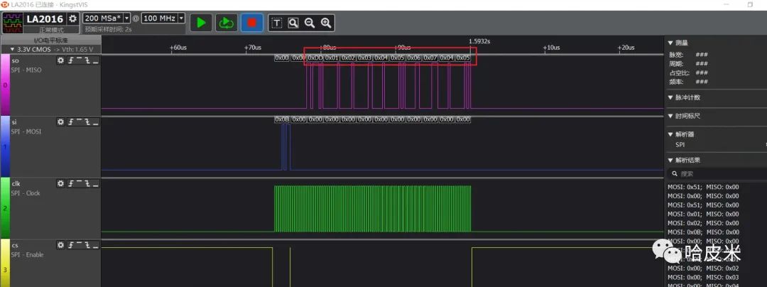
The communication timing for ECR6600 slave consists of cmd dummy data, each occupying one byte. When cmd is 0x0B, it reads data from the slave, and when cmd is 0x51, it writes data to the slave.
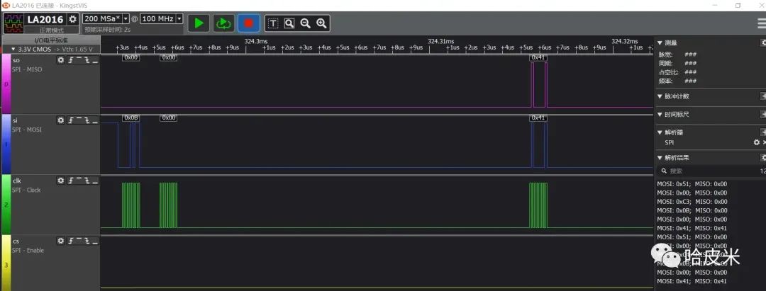
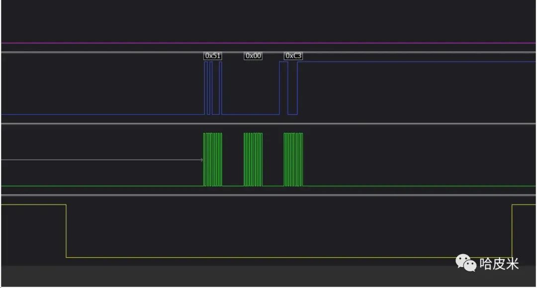
SPI is full-duplex communication, meaning data is sent while receiving. The timing of sending and receiving is controlled by the master. Typically, peripherals must wait for the host to send a command before knowing whether to receive data or respond with data, leading to many command designs effectively becoming half-duplex: in the first half, the host sends a command while the peripheral sends dummy data; in the second half, the peripheral sends a response while the host sends dummy data.
During communication between STM32 SPI master and ECR6600 slave, a characteristic was observed: the clock is not continuous when continuously sending and receiving data. There are gaps in the clock between sending and receiving two bytes of data, which is actually due to the STM32 master not having DMA enabled. When using DMA for transmission, the clock is continuous during continuous send/receive operations.
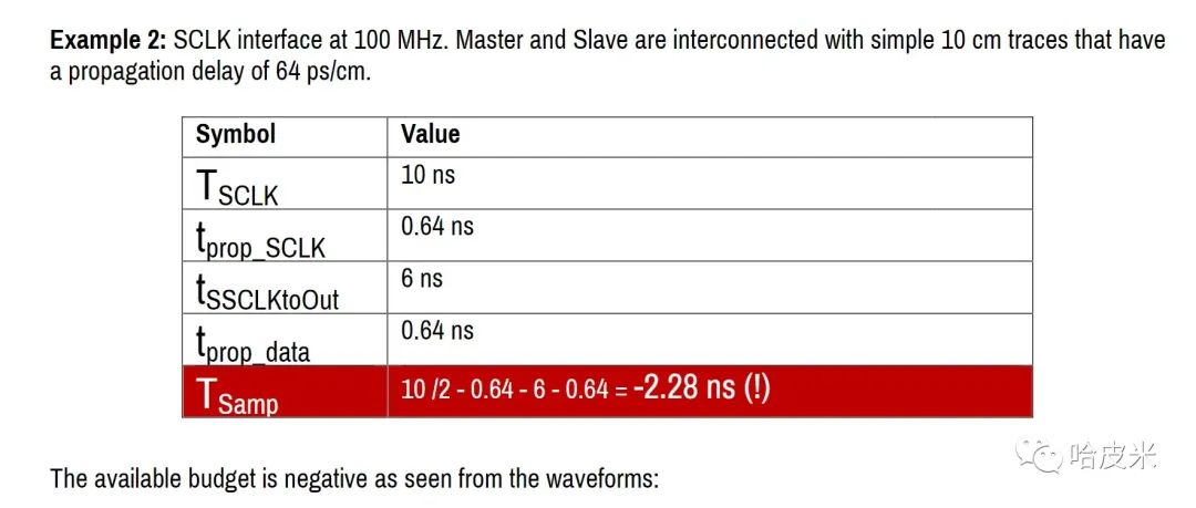
SPI Communication Issues at High Frequencies
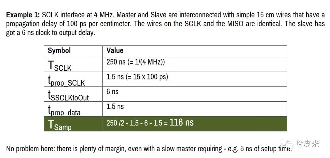
The document “Using-SPI-Protocol-at-100MHz” describes the signal delay paths during SPI communication, with the example of the master reading data from the slave.
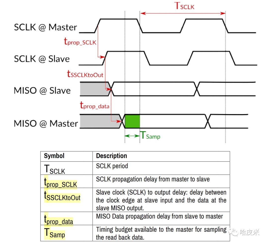
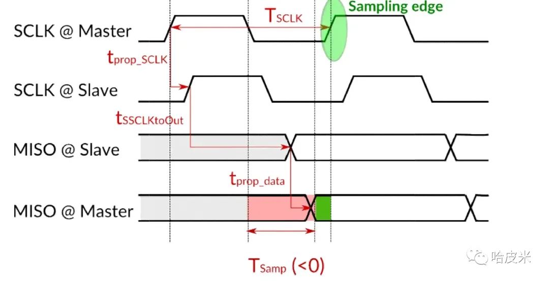
At high frequencies, one must consider the transmission delay of clk between master and slave, the delay from the slave receiving clk to outputting data to the data line (slave’s response speed), and the delay from the slave outputting data to the master’s receiving data line.
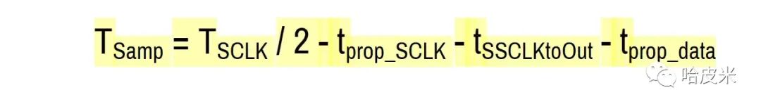
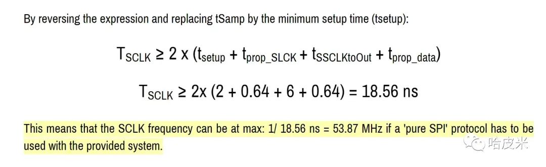
Tsamp is the available time for the master to sample data, calculated as follows:
There are no issues at 4MHz.
However, at 100MHz, the Tsamp time is insufficient. At 100MHz, the clock period is 10ns, requiring the slave to prepare the data to send within 5ns after receiving the master clock signal (to respond), which is practically very difficult to achieve.
How can this issue be resolved?
The document mentions three solutions:
-
Shorten the communication distance between the two, improving the slave’s response speed, which has minimal effect.
-
Reduce frequency. Lowering the frequency is certainly feasible; according to previous examples, the clock frequency should not exceed 53MHz for normal communication.
-
Delay sampling by half or one clock cycle. At 100MHz, the clock period is 10ns; delaying sampling by half a clock cycle allows 10ns for the slave to prepare the data to send, while delaying by one clock cycle allows 15ns for the slave to prepare the data to send.
References
-
High-Frequency Communication Delay Sampling of Spinor/Spinand Flash -
SPI (Serial Peripheral Interface) -
Using-SPI-Protocol-at-100MHz -
Classification of Common SPI LCD Interfaces