Introduction
Proteus is a software designed to automate all stages of electronic device design, including schematic drawing, simulation of processes in analog and digital circuits, printed circuit board layout and routing, as well as editing and expanding component libraries.
The Proteus product suite includes tools for generating circuit schematics (ISIS editor) and tools for designing and routing printed circuit boards (ARES editor). ISIS is used for designing, testing, and debugging circuits. ARES is a PCB application within Proteus for creating printed circuit boards, performing certain CAD functions, and preparing design results for manufacturing. ARES features automatic component layout and routing capabilities, allowing professionals to work in an environment similar to a 3D modeling system, resulting in realistic models of printed circuit boards and their components. ARES tools can generate 3D component models from 2D graphic data in the layout package library. One unique aspect of ISIS is the use of virtual measuring instruments to simulate real-world analog devices. ISIS includes effective tools for visualizing modeling results. Additionally, the program supports the analysis of highly complex analog and digital circuits. The program’s library contains a large number of commonly used electronic components. A comprehensive set of instruments can help measure various quantities, set input signals, and plot graphs. All instruments are designed to closely resemble the appearance of real instruments, making them easy to use and operate.
ISIS provides a variety of virtual measurement tools, the usage of which has been discussed in the literature [2] and [3] . Simulation results can be printed or imported into text or graphic editors for further processing. Figure 1 shows the circuit schematic of the device (Figure 1a), the printed circuit board layout (Figure 1b), and the three-dimensional view (Figure 1c), all drawn using Proteus software.
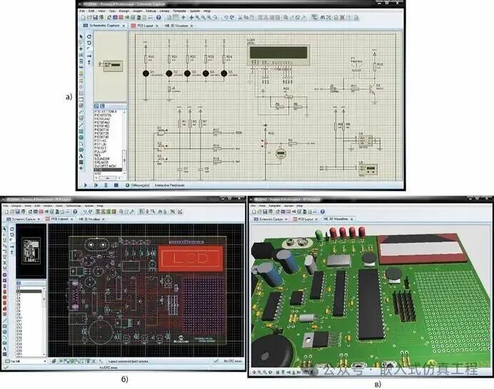
Figure 1. Drawn using Proteus software: a) Circuit schematic; b) Printed circuit board layout; c) Device three-dimensional view
Drawing Electrical Schematics
Proteus is an end-to-end design environment that allows you to create devices from schematic design to printed circuit board manufacturing, controlling every stage of its production.
The first step in designing printed circuit board components in Proteus is to create a circuit schematic, which is created in the ISIS editor. At this stage, necessary components are selected, placed in the drawing workspace, and connected using nets and buses. If necessary, component properties can be modified and text added.
A schematic is a graphical representation of an actual electrical device using conventional graphics and alphanumeric symbols, as well as connections between components. Unlike printed circuit board (PCB) layouts, schematics do not show the physical locations of components but only indicate the terminal interconnections of the graphical symbols of actual components (e.g., integrated circuits) on the PCB. While communication lines can be combined into buses, the line numbers entering and exiting the bus must be clearly marked. In the development of electronic devices, drawing schematics is often a transitional step between the functional diagram development phase and the PCB design phase. GOST 2.701-2008 defines a schematic as “ a diagram that defines the complete composition of components and their connections, usually providing a detailed understanding of the device’s operation “. Complex circuits may contain hundreds of components. Errors in schematic design will inevitably be repeated in all subsequent design documents. Therefore, designers must re-read the schematic to identify errors. Circuit design software greatly simplifies the work of engineers. ISIS is a computer-based circuit editor used to create circuits and simulate various events occurring in actual circuits. The program can be used to assemble basic circuits or develop quite complex circuit designs. Circuits are assembled graphically, significantly simplifying and speeding up the circuit construction process. All components used to assemble the circuit are represented by schematic icons, making it easier for users to find them in the component library.
After creating a blank schematic, the symbols of the required components must be selected from the library for filling. In Proteus , a new schematic project can be created using the “File/New Project“ command. It is important to note that by default, when creating a new project, the “New Project wizard will start (Figure 2). This wizard contains several steps where you need to specify the project name and its location on the computer disk (you can create a project from scratch or use a template provided by the system), specify whether to create an ISIS design (in which case the drawing format needs to be specified) and/or an ARES design, as well as include specific microcontrollers in the project. After completing the wizard, the system will apply the specified settings to generate a new project, which may include a drawing workspace (Figure 3a), PCB outline (Figure 3b), and a program code template for the microcontroller (Figure 3c). It is important to note that during component design, the schematic design, PCB design, device 3D view, and program code editor (if the circuit uses a microcontroller) can be opened simultaneously. Additionally, each editor will create a separate tab.
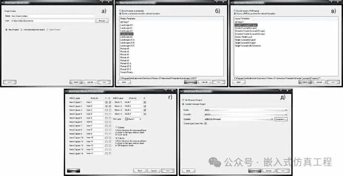
Figure 2. Steps to create a new project using the “New Project Wizard“: a) Name and select project location; b) Create ISIS design; c) Create ARES design; d) Use PCB layers; e) Include microcontrollers in the project
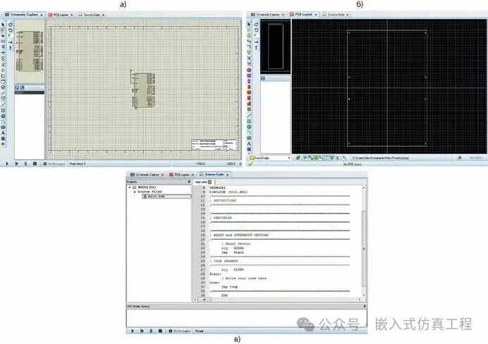
Figure 3. Results of the new project wizard: a) Drawing workspace; b) Printed circuit board outline; c) Blank program code for the microcontroller
Placement of Component Symbols on the Schematic
To select components for subsequent placement in the program workspace, this must be done in the “Select Device“ window (Figure 4). This window can be opened using the context menu command “Place/Component/From Library“ or by pressing the “Device“ button on the panel (by default, this panel is located on the left side of the program and contains a list of components available in the project). To open this panel, press the ISIS editor’s left toolbar button labeled “Component Mode“.
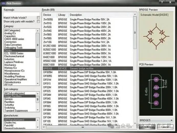
Figure 4. Select Device Window
Once a component is selected, its symbol will appear in the “Preview“ field. The component’s package will be displayed in the “PCB Preview“ field. If the desired component has multiple packages, all possible options will be displayed in the dropdown list below the “PCB Preview“ field for selection. To place the selected component on the schematic, click the “OK“ button in the Select Device window. The window will then close, and the component symbol will attach to the mouse cursor, allowing you to place the symbol on the schematic (clicking at the desired location on the schematic). For more detailed information on placing component symbols on the schematic, see [4].
Connecting Component Symbols in the Schematic
Wires and buses are used for communication between various components in the circuit.Proteus does not have a specific command for adding new circuits to the circuit.
To wire between components, move the mouse cursor to the terminal of the component where the wire starts, click the left mouse button, and then drag the wire in the desired direction. Clicking the left mouse button in the project workspace creates circuit bends. To complete the wiring, move the mouse cursor to the next terminal and click the left mouse button. The wiring is complete. If the circuit contains electrical nodes (i.e., connecting more than two component terminals), another wire can be connected along the entire length of the wire to the circuit. This will create an electrical node at that position.
To connect symbol contacts to the circuit, move the cursor to the selected contact to be connected, click the left mouse button, and then drag the cursor to the connection point with another circuit. Then, click the left mouse button at that connection point— the system will create a node at the connection between the new circuit and the existing circuit.
Buses are used when multiple circuits share the same path. Buses group circuits together, making the circuit diagram easier to read. To add a bus to the circuit diagram, use the “Bus Mode“ button on the left toolbar. Buses are drawn on the circuit diagram using the mouse cursor and are displayed as a thick blue line. Connecting to a bus is the same as connecting to a conductor but does not create an electrical node.
Once the circuit is assembled and all necessary components are connected, you can simulate it using the “Run Simulation“ button located in the lower left corner of the program window. To temporarily pause the simulation, use the “Pause Simulation“ button; if the simulation has stopped, use the “Restart from Time0 “ button (also located in the lower left corner of the program window). To stop the simulation, use the “Stop Simulation“ button. Simulation results can be printed or imported into graphic editors for further processing.
You can save the developed scheme using the “File/Save Project“ and “File/Save Project As“ commands.
Managing Project Workspace and Chart Object Colors
The ISIS editor allows designers to control the colors of the program workspace. By default, the workspace color is light gray, but it can be easily changed. This can be done in the “Edit Design Defaults“ window (Figure 5) in the “Paper Color“ field, which can be accessed through the “Template/Set Design Colors“ main menu command. This window also allows you to set the colors of the following schematic objects:
- Grid Color— Grid;
- Workspace Frame Color— Frame for selecting the drawing workspace;
- World Box Color– Origin;
- Highlight Color— Selected components in the circuit;
- Drag Color— The color of components and animated objects (animations) when dragged with the mouse in the project workspace, including the color of logic levels:
- Logic 1 Color– Logic unit;
- Logic0 Color– Logic zero;
- Logic? Color– Uncertain state;
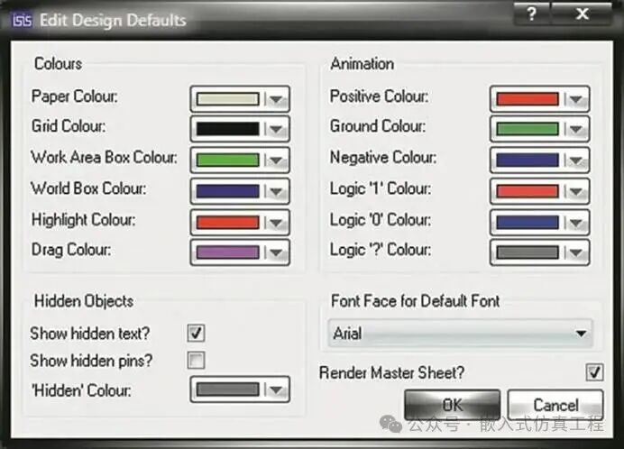
Figure 5. Edit Design Defaults Window
You can customize colors by clicking the color icon next to the name of the object you want to change, then selecting the desired color from the palette. The color icon reflects the actual color of the chart object. You can also set the font for drawing text in the “Edit Design Defaults“ window. This can be done by selecting the desired font from the dropdown list in the “Default Font“ field. To apply the changes, click “OK“.
Creating Custom Text Styles
In ISIS , you can create your own text styles or edit existing styles used to display text on the drawing (pin names, component pin numbers, network names, text labels, etc.). All these operations are performed in the “Edit Global Text Styles“ window (Figure 6), which can be opened via the main menu command “Template/Set Text Styles“.
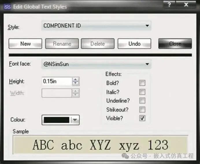
Figure 6. Edit Global Text Styles Window
To create a new style, click the “New“ button in this window, then in the opened “Create New Text Style“ window (Figure 7), enter the name of the style you want to create in the “New Style Name“ field, and then click “OK“. The added style will immediately appear in the list of existing text styles in the “Edit Global Text Styles“ window under the “Style“ field. Now, to configure the settings of the new style, click the style name in the dropdown list of the “Style“ field, and specify the following:
- Font – To do this, select the desired font from the dropdown list in the “Font“ field (this list displays all system fonts in the C:\Windows\Fonts folder);
- Font Size: Height (Height field) and Width (Width field);
- Font Style: If you want to bold the font, check the “Bold“ checkbox; otherwise, leave it unchecked; if you want to display the text in italics, check the “Italic“ checkbox;
- Strikethrough – To display the font with a strikethrough, you need to check the “Strikethrough“ checkbox;
- Underline – To do this, you need to check the “Underline“ checkbox;
- Visibility – Set by checking/unchecking the “Visible“ checkbox;
- Color – Set the color by clicking the color icon in the “Color“ field and selecting the desired color from the opened palette.
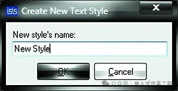
Figure 7. Create New Text Style Window
Once all parameter configurations are complete, you can preview the newly created style in the “Example“ window (i.e., the preview window for the text style you are creating). If you are satisfied with the result, click “Close“ to exit the “Edit Global Text Styles“ settings window and return to the project. If you are not satisfied, try adjusting the text style parameters until you achieve the desired result. The following commands can be applied to custom text styles:
- Rename (Rename button);
- Delete (Delete button).
Editing the parameters of existing text styles is done in a similar manner.
Creating and Editing Graphical Styles of Chart Elements
The display styles of schematic components (component symbols, nets, buses, component pins, etc.) can be edited, and custom styles can be created if necessary. All related operations are performed in the “Edit Global Graphical Styles“ window (Figure 8), which can be opened via the “Template/Set Graphical Styles“ main menu command. Let’s take a closer look at the “Edit Global Graphical Styles“ window. At the top of the window is the “Style“ menu, which displays all existing styles of schematic graphical elements.“Style“ menu is followed by a series of buttons that can be used to:
- Add New— Create a new graphical style;
- Rename— Rename an existing style;
- Delete— Delete a style;
- Undo— Cancel the user’s executed action;
- Close— Close the “Edit Global Graphical Styles” window.
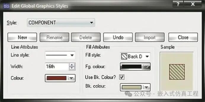
Figure 8. Edit Global Graphical Styles Window
After creating a new style, it will immediately appear in the list of available graphical styles in the “Style“ field. To configure the parameters of the new style or change the parameters of an existing style, click the style name in the dropdown list of the “Style“ field and specify the following:
- Line Style (Line Style field);
- Line Thickness (Width field);
- Line Color (Color field);
- Fill Style (Fill Style field);
- Fill Color (Color field);
- Background Color (checkbox “Use Background Color“);
- Background Color (Color).
“Example“ window is used to preview the graphical style being created. If you are satisfied with the result, click “Close“ to exit the “Edit Global Graphical Styles“ settings window and return to the project. If you are not satisfied, try adjusting the style parameters until you achieve the desired result. Figure 9 shows a part of the chart before and after setting custom text and graphical style settings.
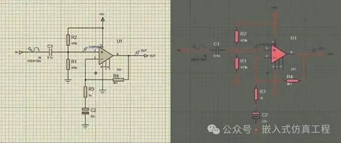
Figure 9. Chart before and after setting text style and graphical element custom settings
Naming Wire Labels
For readability, you can assign a name to each network in the diagram. To do this, right-click on the wire and select “Place Wire Label“ from the context menu. This will open the “Edit Wire Label“ window. In this window, you can enter the network name in the “Label“ tab (Figure 10a) in the “String“ field, or select a name from the dropdown list in the same field. In the “Rotation“ and “Alignment“ fields, you can set the direction and alignment of the text relative to the wire by moving the radio buttons to the desired position.
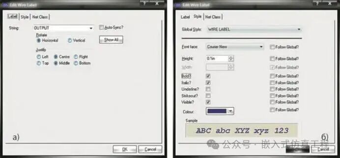
Figure 10. Edit Wire Label Window: a) Label Tab; b) Style Tab
You can also open the “Edit Wire Label“ window by clicking the ISIS editor’s left toolbar icon labeled “Wire Label Mode“ icon, hovering the mouse cursor over the wire to be labeled (a cross will appear), and then clicking the left mouse button. This will open the “Edit Wire Label“ dialog.
The visibility of network names in the chart is set by the context menu commands “Show All Wire Labels“ and “Hide All Wire Labels“.
You can also easily customize the display style of network names in the schematic in the “Edit Wire Label“ window. This can be done in the “Style“ tab (Figure 10b). To apply the changes made in the “Edit Wire Label“ window, click “OK“. Figure 11 shows a network with an assigned name.
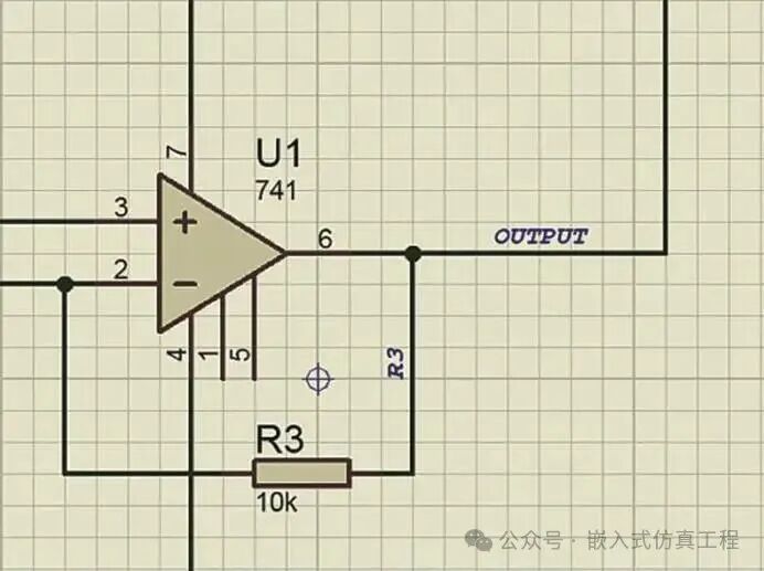
Figure 11
You can also name wires that are “disconnected,” meaning one end is connected to a component pin while the other end is not connected. However, if the wire is labeled, the system will connect it to the circuit with the same label (name). This method is very useful when the circuit density is high and long-distance wiring is not possible. Additionally, this method also facilitates connecting the pins of discrete components to power and assigning them VCC and GND labels.
Setting Labels for Graphics
Labels are an essential part of schematic documentation. The appearance of labels is determined by the font (i.e., the style of letters and numbers). To add a label to the schematic, click the ISIS editor’s left toolbar icon labeled “2D Graphics Text Mode“. In the opened “Graphics“ panel, select “2D Graphics“, and then click on the location in the chart where the label should be placed.
After that, the “Edit 2D Graphics Text“ window (Figure 12) will open, where you can specify:
- Label Font (Font field);
- Font Size: Height (Height field) and Width (Width field);
- Font Style: Italic ( Italic checkbox), Bold (Bold checkbox);
- Underline Text (check the checkbox Underline);
- Strikethrough Text (Strikethrough checkbox);
- Text Color (Color field);
- Text Alignment (Alignment field).
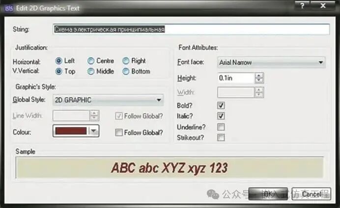
Figure 12. Edit 2D Graphics Text Window
In the “String“ field, enter the desired text. Changes to the text font settings will be displayed in the “Edit 2D Graphics Text“ window’s bottom “Example“ preview. If you are satisfied with the text, click “OK“. The text will be placed in the drawing area (Figure 13).
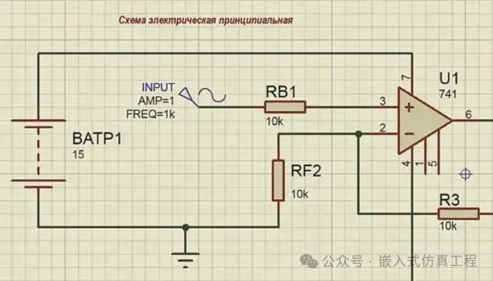
Figure 13. Text Annotation in the Drawing Area
To delete a text label, right-click on the text block in the chart and select “Delete Object“ from the context menu. You can also delete a text label using the Delete key on the keyboard. To do this, click on the text label with the left mouse button and then press the Delete key.
Printing Circuit Schematics
Once the circuit schematic is complete, you may need to print it. You can print the entire design or schematic using the “File/Print Design“ command in the main menu. The ISIS editor also allows you to print specific areas of the drawing. To do this, select “File/Mark Output Area“ from the main menu, use the mouse to select the desired area in the schematic (the mouse cursor will change to a marker, and the selection will be outlined with a dashed box), and then click the endpoints of the selection. The area to be printed will be highlighted in gray (Figure 14).
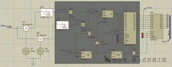
Figure 14. Area on the Drawing for Printing
After running the “File/Print Design“ main menu command, the “Print Design“ window will open (Figure 15), where you can set the following:
- Page Orientation field— Page orientation: Portrait (vertical), Landscape (horizontal);
- Number of Copies field— The number of copies of the document to print;
- “Content to Print” field— Output options, in this field, by setting the switch to the desired position, you can determine what content to send to print: Marked Area – Selected part of the graphic, Current Graphic – Current graphic, current Sheet – Current sheet, All Sheets – Entire unfolded drawing;
- Scale field— The scale of the chart output on the page;
- Color Printing checkbox— Color printing of the document;
- Printer button— Printer settings.
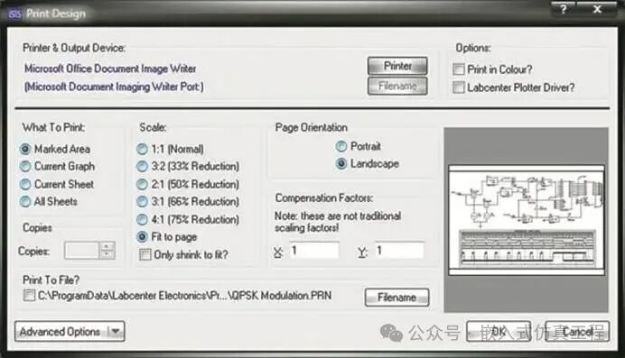
Figure 15. Print Design Window
Printing can be done on paper or saved to a file. To print the chart to a printer (plotter), select the printer to print from the dropdown list in the “Printer“ panel in the “Print Settings“ window (opened by clicking the “Print“ button) from the “Name“ field’s dropdown list, and then click the “Properties“ button to configure the printer’s print settings. Figure 16 shows the “Print Settings“ window (where parameters for printing the chart on the printer are configured) and the “Printer Properties“ window (opened after clicking the “Properties“ button). To print the graphic to a file, select “Microsoft Office Document Image Writer from the dropdown list in the “Printer“ panel, and then click the “Properties“ button. In the opened “Microsoft Office Document Image Writer Properties“ window’s “Advanced“ tab, specify the file extension and image resolution for the chart to be saved. In the “Default Folder“ field, specify the location where the created chart file will be saved. To apply the changes, click “OK“. Figure 17 shows the “Print Settings“ window, where parameters for printing the chart to a file are configured, as well as the “Microsoft Office Document Image Writer Properties“ window.
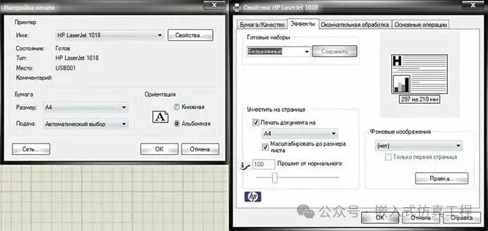
Figure 16. Print Preferences and Printer Properties Window
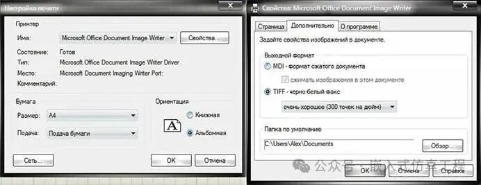
Figure 17. “Print Preferences” and “Microsoft Office Document Image Writer Properties“ Window
In the “Print Design“ window’s lower right corner, there is a preview window showing the graphic ready for printing. If you are satisfied with the design, click the “Print Design“ button in the lower right corner of the window. Otherwise, click the “Cancel“ button to return to the drawing workspace. After making the necessary changes, you can return to the “Print Design“ window, and if you are satisfied with the result, you can print the chart.
If you choose to print to a file, clicking the “Print Design“ button in the window will open the “Save Document“ dialog. In this dialog, you can specify the file name, type, and location on the computer disk, and then click “Save“. The graphic will be saved in the *.tiff file format in the specified folder(Figure 18).
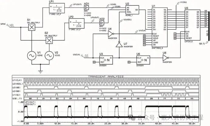
Figure 18. Result of Printing the Graphic to a File
Conclusion
Proteus is a modern electronic circuit simulation program that provides a virtual laboratory, including measuring instruments and a rich library of electronic components. These tools allow engineers to verify whether the designed devices meet design specifications, even when using components with less than ideal characteristics. Proteus can automate all stages of electronic device design, including schematic drawing, simulation of analog and digital circuit processes, printed circuit board layout and routing, as well as editing and expanding component libraries.
Understanding the algorithms implemented in Proteus and the principles of building electronic component models is crucial for effectively using Proteus. Improper application of component models, configurations, and computational algorithms can lead to erroneous modeling results.
Welcome to follow (for operational reference articles: Follow the public account and send messages for operations), click the blue text at the top “Embedded Simulation Engineering” or long press to identify the QR code to follow