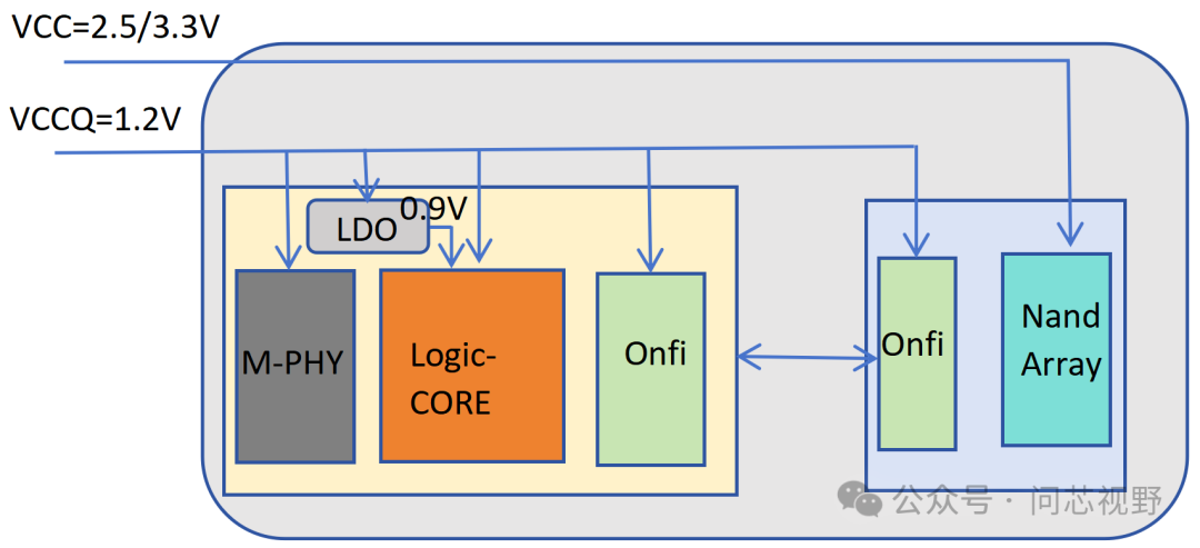
The NAND Controller IC is the brain of NAND, managing the interaction between NAND and external SoC. It supports standard interfaces (such as SATA, PCIe/NVMe, USB, UFS, etc.) and implements functions such as wear leveling, bad block management, garbage collection, ECC, read/write cache performance, write protection, and address mapping. However, since it is packaged together with NAND chips as storage chips like UFS/EMMC/SSD, the specifications of the controller are rarely focused on by application developers. They only look at the specifications of the storage chip without understanding the internal details. The controller has become knowledge that is only known to a few in the Flash professional field, with relevant information available only to flash manufacturers, controller chip designers, and module manufacturers. This article provides a simple introduction to some aspects of the controller to help those outside the field understand. Chip Block Diagram:Three main functional blocks:Host Controller, also known as Front-End (FE): Mainly handles interface protocols, command processing, data transmission, FFU upgrades, etc.;FTL (Flash Translation Layer): Garbage collection, cache management, security, wear leveling, controller system, physical address mapping, code, logs, etc.;Flash Controller: Read, write, erase, interface protocols, ECC, NAND management, etc.;Taking the Marvell SSD controller as an example: Observing its chip architecture, there are two CPUs with different specifications, one for handling HC and FW, and the other for handling FC. Due to the complexity of the firmware, there are many internal modules, including data interaction between the two CPUs and buses, which we cannot know;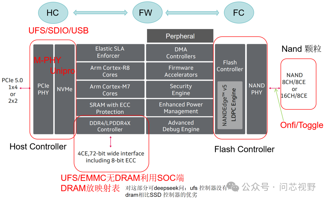 UFS 3.1/4.1 Power Supply:
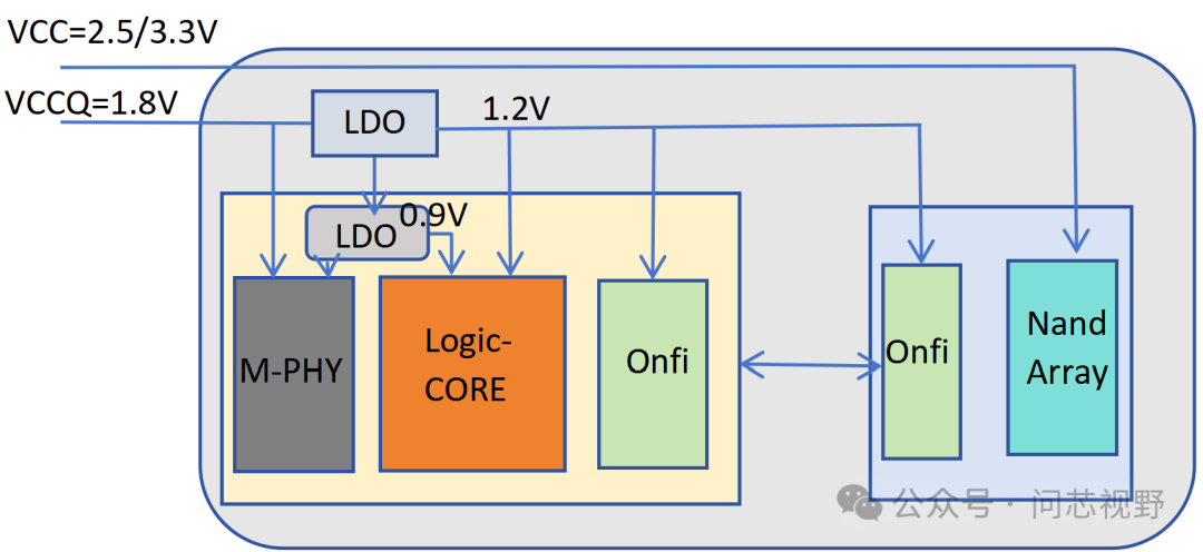
 UFS 2.2 Power Supply: Since the interface RESET/REF_CLK, etc. are at 1.8V, but the internal ONFI is at 1.2V, an LDO is needed for level shifting;
 Key Parameters of the Controller:: The selection of the controller is mainly done by the flash manufacturers or memory module manufacturers. Since the chip and firmware algorithms are combined, the selection not only considers chip performance but also the optimization of the firmware and its compatibility with the target end product. Factors such as size, operating temperature, support for flash chips (different NAND manufacturers, TLC/QLC, etc.), capacity, QoS, reliability, interface protocol support, performance metrics, power consumption metrics, error correction performance, unique algorithms, and process technology are all important.The following image shows the key indicators of Marvell chips:
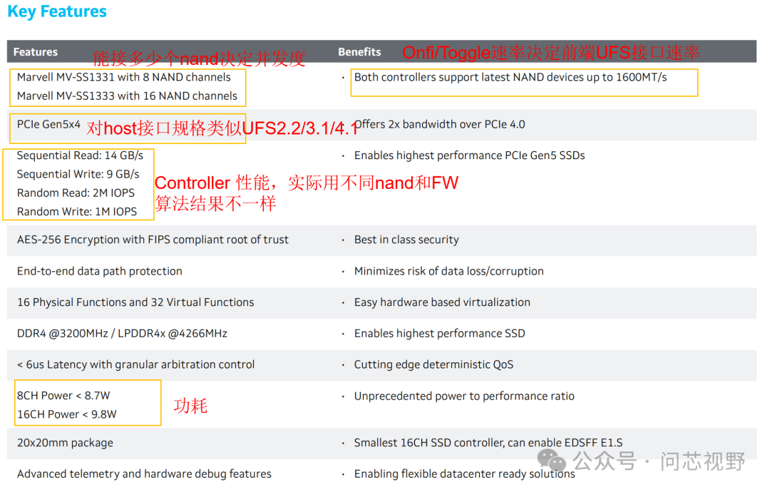 Reference for Marvell SSD controller MV-SS1331 product introduction:https://cn.marvell.com/content/dam/marvell/en/public-collateral/storage/marvell-ssd-mv-ss1331-1333-product-brief.pdf