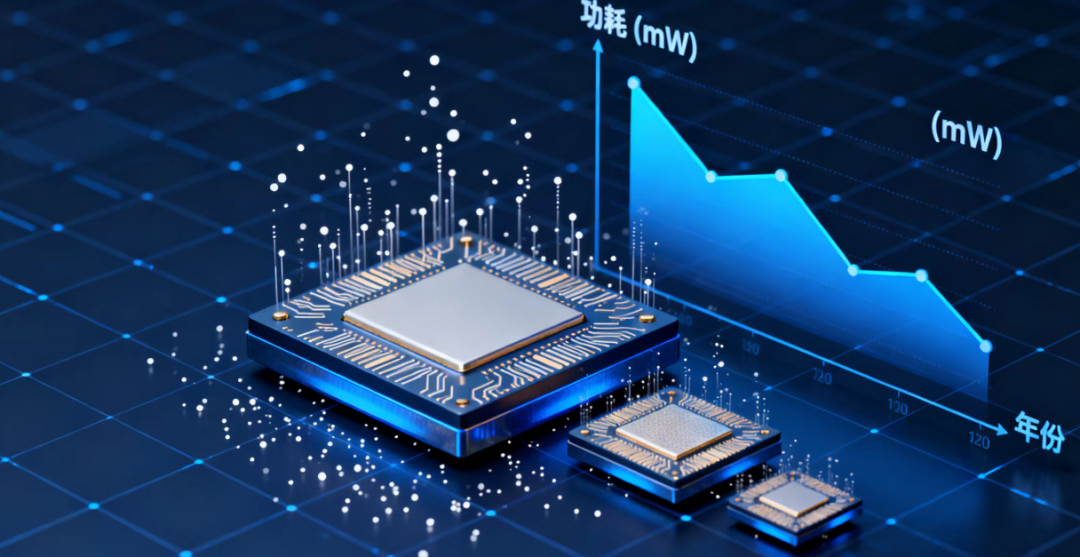
 This is the 361th content shared by the platform.
 Low-power technology for chips is one of the cornerstones of the modern semiconductor industry, and its development is closely related to our digital lives. Below, the platform will systematically elaborate on the evolution of low-power technology for chips from three aspects: origin, development, and outlook.

Original
01. Origin
Passive Response Driven by Physical Laws
 The origin of low-power technology was not an active pursuit but was driven by two core factors:
Increased Integration and Frequency Leading to Power Consumption Surge
With the advancement of Moore’s Law, the number of transistors has increased exponentially, and the clock frequency of chips has also risen. According to the dynamic power formula P = α * C * V² * f (where P is power consumption, C is load capacitance, V is voltage, and f is frequency), power consumption has surged.High power consumption has brought severe challenges:
- Heat Issues: Excessive chip temperature can lead to instability, shortened lifespan, or even burnout.
- Battery Life Issues: For early mobile devices (such as laptops), high power consumption severely limited battery life.
- Cost Issues: More expensive cooling systems and larger batteries are required, increasing product costs and size.
The End of Dennard Scaling Law:
Before 2000, Dennard scaling law (the reduction of transistor size while maintaining power density) was effective.
However, entering the deep submicron era, the leakage current of transistors (static power consumption) increased sharply, and Dennard’s law gradually failed. This means that even as transistors shrink, power consumption per unit area can no longer decrease, forming a “power wall.”
Key Technologies of This Period
-
Reducing Operating Voltage (V): From 5V to 3.3V, and then to 1.xV, this is the most effective means of reducing dynamic power consumption.
-
Clock Gating: When a circuit module is not in operation, its clock signal is cut off, eliminating the dynamic power consumption of that module. This was the earliest architectural low-power design method.
-
Process Improvements: By reducing transistor size, load capacitance (C) is lowered, indirectly reducing power consumption.
The core feature: The technology of this stage (1970-1990) was mainly passive and local, aimed at solving the urgent problem of “heat,” and had not yet formed a systematic low-power design methodology.
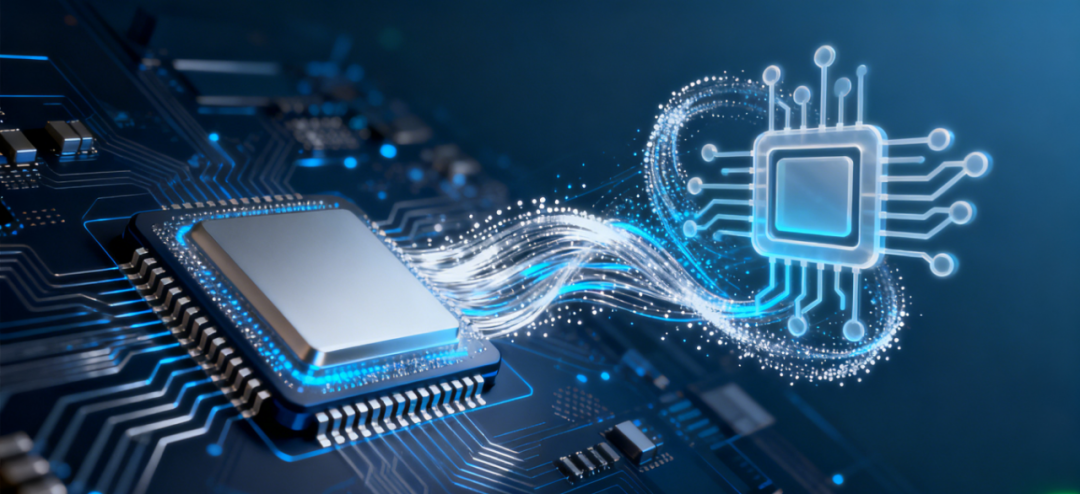 (Image source: Internet)

Evolution
02. Development
Active Innovation and System-Level Methodology
 The timeline of this period is from 1990 to around 2010, with the explosion of the mobile internet era (represented by smartphones) and portable computing devices, where power consumption directly determines product competitiveness.Low-power technology has transitioned from an “optional” to a “mandatory” requirement, entering an active and systematic development stage.
Multiple Voltage Domains
Different modules of the chip operate at different voltages based on performance requirements. High-performance cores use high voltage, while low-performance or standby modules use low voltage, even ultra-low voltage.
Power Gating
More thorough than clock gating, it directly cuts off the power supply to idle modules, thus eliminating both dynamic and static power consumption. This requires a complex power management architecture and state save/recovery mechanisms.
Power Management Technologies
From hardware to software collaborative design.
- Dynamic Voltage and Frequency Scaling (DVFS): The system dynamically adjusts the processor’s voltage and frequency based on real-time computational load. When the load is low, it immediately reduces frequency and voltage to save power.
- Adaptive Voltage Scaling (AVS): More advanced than DVFS, it monitors the actual process variations and temperature of the chip, making real-time fine-tuning of voltage to minimize power consumption while ensuring functionality.
Asynchronous Circuits
Attempts to break free from the constraints of a global clock, communicating through handshake protocols, which can avoid the significant power consumption caused by clock trees.However, due to design complexity and insufficient EDA tool support, it has not become mainstream but has applications in certain specific fields.
Low-Power Processes
- Foundries have introduced process nodes specifically optimized for ultra-low power scenarios (such as ULL, HPC+, etc.), improving power performance by optimizing transistor structures (such as the introduction of FinFETs, which significantly reduce leakage current).
-
Multi-threshold Voltage Libraries: In design, both high-threshold voltage (HVT) transistors (low leakage, slow speed) and low-threshold voltage (LVT) transistors (high leakage, fast speed) are used simultaneously, ensuring performance with LVT on critical paths and reducing leakage with HVT on non-critical paths.
-
FD-SOI and other technologies: Compared to traditional bulk CMOS processes, FD-SOI has lower leakage current and better back-bias control, making it very suitable for ultra-low power applications.
The core feature: A system-level low-power design process represented by standards such as UPF/CPF has formed. Power consumption has become a core design metric alongside performance and area, permeating the entire process from architectural design to physical implementation.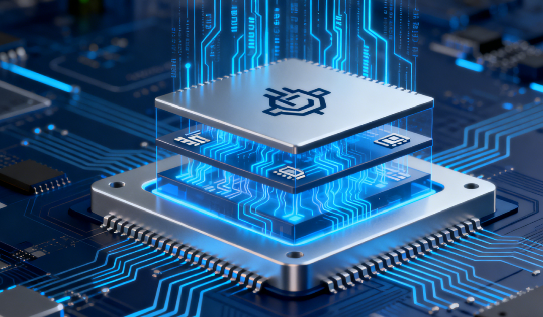 (Image source: Internet)

Outlook
03. Outlook
AI-Driven and Cutting-Edge Exploration
 Currently, the world is entering the era of intelligent everything (AIoT) and artificial intelligence (AI), with explosive growth in computing power demand. However, constrained by the “power wall” and “memory wall,” as well as the slowdown of Moore’s Law, low-power technology faces unprecedented challenges and opportunities. Future development will be more multidimensional, intelligent, and interdisciplinary.
Architecture for Specific Domains
It is difficult to improve the energy efficiency of general-purpose CPUs; the future trend is to design dedicated architectures for specific workloads (such as AI inference, image processing).
- DSA: Domain-Specific Architectures achieve extremely high computational efficiency with extremely low power consumption through hardware customization.
- In-Memory Computing: Completely overturns the von Neumann architecture by embedding computing units within memory, greatly reducing the power consumption of data movement (data movement is the main source of power consumption in AI chips).
- Heterogeneous Computing: Efficiently collaborates different architectures of processors such as CPU, GPU, and NPU, allowing suitable tasks to run on appropriate cores to achieve optimal system-level energy efficiency.
New Devices and New Materials:
- Gate-All-Around Transistors: Following FinFETs, GAA transistors (such as Samsung’s MBCFET) can provide better channel control and lower leakage current.
- Two-Dimensional Materials: Such as graphene and transition metal dichalcogenides, are expected to create thinner and better conductive channels, further reducing device size and power consumption.
- Ultra-Low Power Devices: Such as negative capacitance transistors and tunnel field-effect transistors, aim to break through the subthreshold swing limitations of traditional CMOS devices to operate at extremely low voltages.
Near/Subthreshold Computing
Allows chips to operate in the region close to or below the turn-on voltage of transistors, which can reduce power consumption by an order of magnitude.However, the challenge lies in poor stability and slow speed, requiring robust error tolerance and compensation circuit technologies. This has great potential in ultra-low power scenarios such as energy harvesting.
AI-Powered Power Optimization:
- Design Phase: Utilize machine learning algorithms to quickly predict and optimize power consumption during chip layout, clock tree synthesis, and other stages, replacing traditional time-consuming simulation iterations.
- Operating Phase: Integrate power management units within the chip, using AI algorithms to learn and predict workloads in real-time, achieving more refined and proactive DVFS and power gating.
System-Level and Software-Level Collaboration
Transitioning from “chip-level low power” to “system-level low power” and “algorithm-level low power.”
- Algorithm Optimization: Design low-power AI algorithms such as sparsification and quantization to fundamentally reduce computational load and memory access.
- Hardware-Software Co-Design: Deep collaboration between compilers, operating systems, and hardware for task scheduling, power management, etc., to maximize energy efficiency.
 (Image source: Internet)

Summary
4. Summary

The evolution path of low-power technology for chips is clear:
-
From Passive to Active: Transitioning from solving heat issues to becoming a key competitive factor for products.
-
From Local to System: Evolving from optimizing individual transistors and modules to full-link collaborative optimization at the chip, system, and algorithm levels.
-
From General to Specific: Shifting from improving the energy efficiency of general-purpose processors to customizing architectures for extreme efficiency for specific tasks.
-
From Micro to Macro: While exploring microscopic technologies such as new devices, there is also a greater focus on macro-level innovations such as architecture and software.
Looking to the future, low-power technology will be a key bottleneck and core driving force for the implementation of cutting-edge technologies such as artificial intelligence, the metaverse, and the Internet of Things. It is no longer just a topic for circuit designers but a frontier interdisciplinary field that requires collaboration among architects, algorithm engineers, software developers, and even physicists and materials scientists.
Previous Recommendations >
Previous articles
High-Precision Switch New Choice: TMUX1308 Chip, Outstanding Low-Power Performance!

8GHz Low Noise, Low Power Fully Differential Wideband Amplifier Using Complementary BiCMOS – LMH5401
Adesto 16-bit SAR-ADC Chip AD4001 – Reducing Signal Chain Power Consumption, Lowering Signal Chain Complexity, and Achieving Higher Channel Density

AD9653: Four-Channel High-Precision ADC, Wide Bandwidth + Low Power + Flexible Control, Fully Competent for Medical / Imaging / Communication