Code Analysis
The LTC2308 communicates via a standard 4-wire SPI digital interface. The LTC2308 analog-to-digital converter (ADC) chip has 8 ADC channels and a resolution of 12 bits, with an input signal clock frequency range not exceeding 500 KHz. According to the Nyquist sampling theorem, it is recommended that the input signal be below 250 KHz.
The following is the LTC2308 circuit on the DE10-Standard development board:
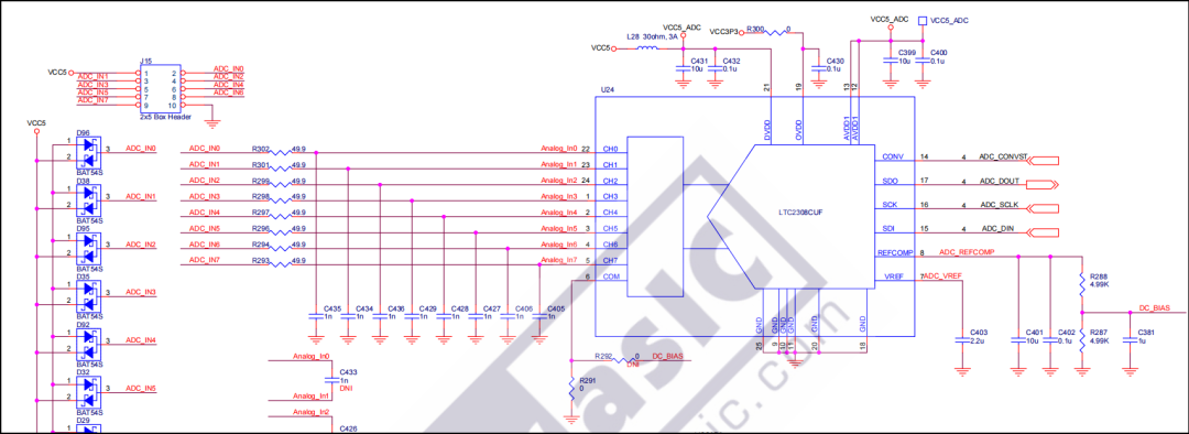
From the circuit diagram, it can be seen that the COM pin of the LTC2308 is connected to GND, indicating that the LTC2308 on the current DE10-Standard development board is configured for unipolar input.
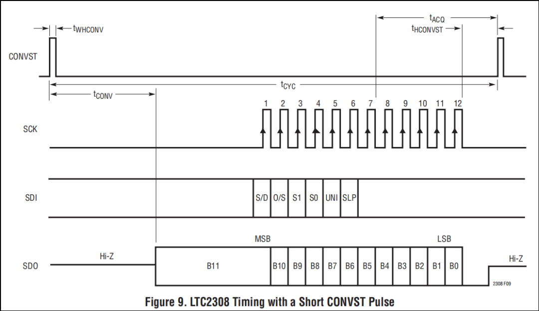
The timing diagram for the LTC2308 SPI protocol is as follows:
The block diagram of the LTC2308 control module (adc_ltc2308.v) is as follows:
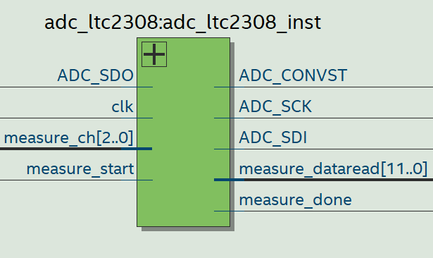
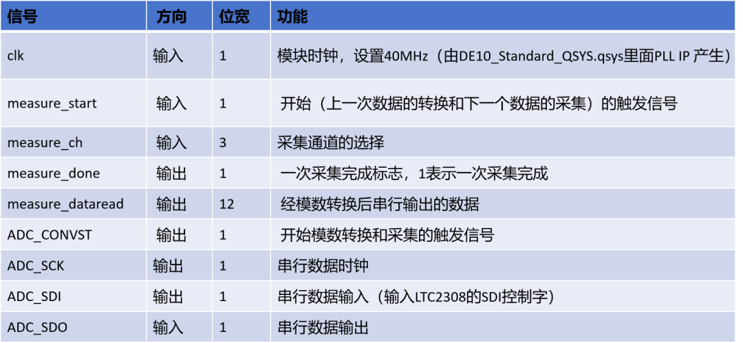
The signal list is as follows:
Module parameter design:
The DE10-Standard development board manual (DE10-Standard_User_manual.pdf) mentions that to set a sampling rate of 100 Ksps, simply set tHCONVST to 320. Next, let’s see how this value of 320 is calculated.
According to the LTC2308 datasheet, we know that its maximum sampling rate is 500 ksps, SCK can reach a maximum of 40 MHz, and the typical value of tCONV is 1.3 us, with a maximum value of 1.6 us. The time period for 100 Ksps is 10 us, while the time period for 40 MHz is 25 ns. The entire process (including conversion and sampling) takes up 10 us / 25 ns = 400 cycles. 1.6 us / 25 ns = 64, so tCONV occupies at most 64 clock cycles.
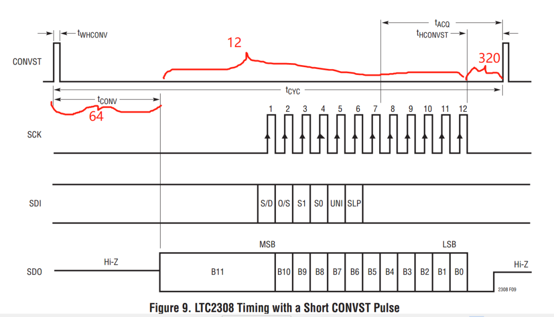
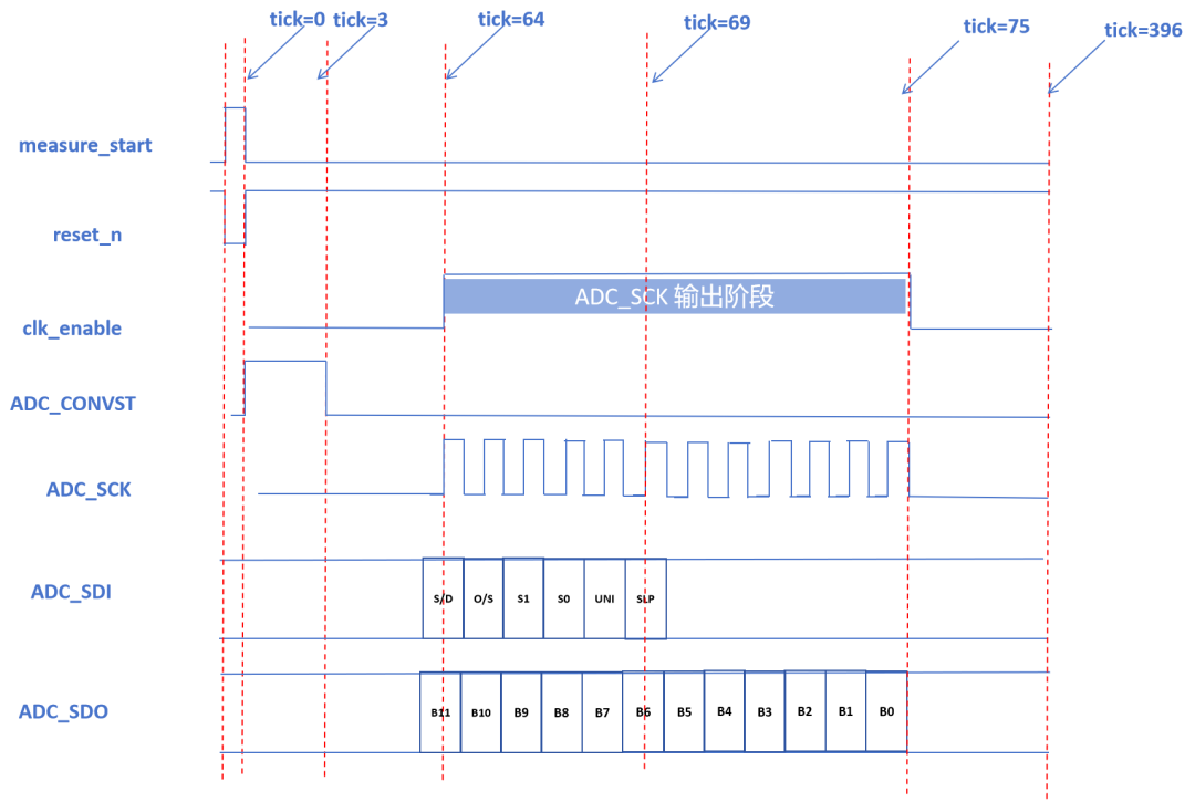
Based on the timing diagram and the code, 64 + 12 + 320 = 396, which is approximately 400.
The parameter settings in the adc_ltc2308.v code are as follows:
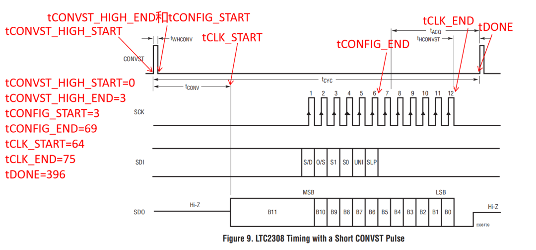
Code explanation:
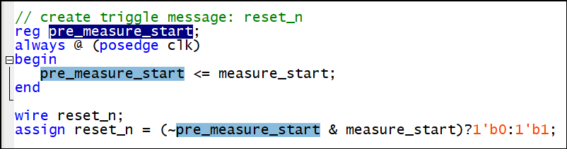
Once the rising edge of the trigger signal measure_start is detected, the system reset signal of the adc_ltc2308 module is set to 0:
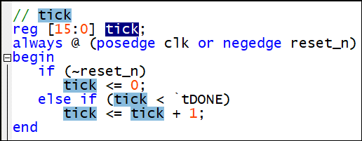
A counter is designed to count the number of clock cycles required for a complete conversion and acquisition process of the LTC2308:
Output the ADC_CONVST signal (which marks the tWHCONV time period):

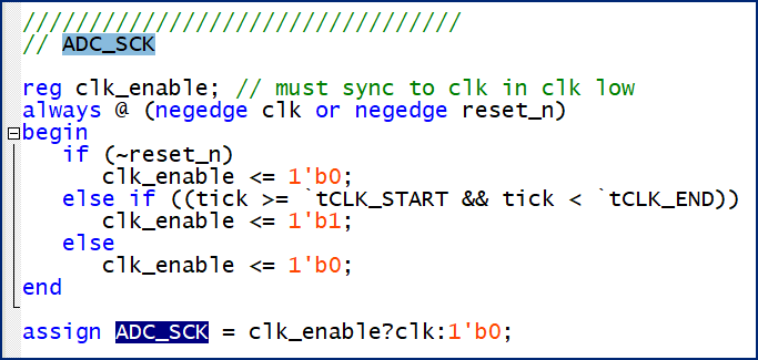
Output the SCK clock, with the ADC_SCK period being 40 MHz, but only 12 cycles are output each time, with the rest of the time outputting a low level of 0:
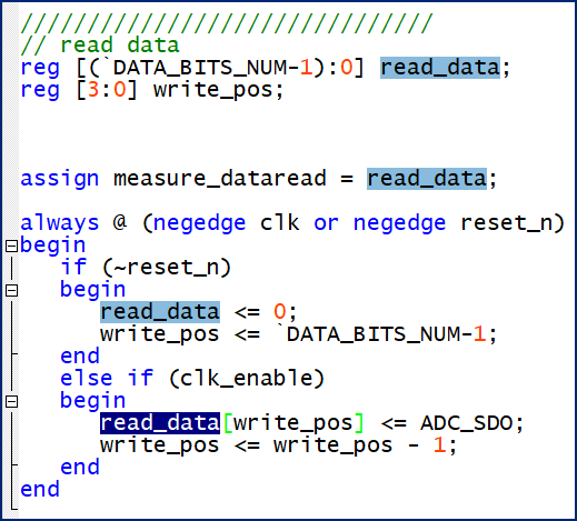
At the falling edge of clk, the completed conversion data is written to the register:
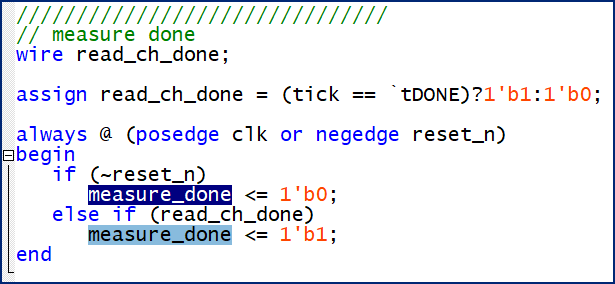
measure_done is the flag for the completion of one acquisition. Each time the rising edge of the LTC2308 trigger signal is detected, the measure_done signal is set to 0, and after one acquisition is completed, it is set to 1:
measure_done is the flag for the completion of conversion + transmission + sampling. The measure_done signal is cleared to 0 when starting a new round of sampling and set to 1 after transmission is complete:
reset_n, clk_enable, measure_done, ADC_CONVST, and ADC_SCK signal waveforms are marked as follows:
Based on the input (measure_ch), different configuration words are stored in the register config_cmd:
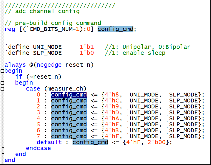
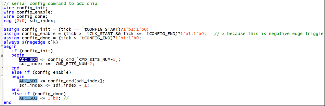
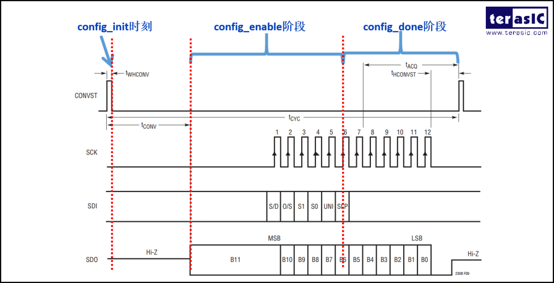
Then, according to the LTC2308 timing diagram, the three stages of the configuration word are marked (three states): config_init (configuration initialization time), config_enable (configurable time), and config_done (configuration completion time).
config_init (configuration initialization time): In the initial state, the high byte of the configuration word is assigned to ADC_SDI.
config_enable (configurable time): The remaining 5 bits of the configuration word are assigned to ADC_SDI one by one.
config_done (configuration completion time): In the configuration completion stage, 0 is assigned to ADC_SDI.
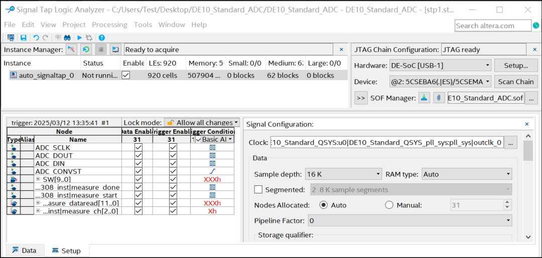
Open the ~DE10_Standard_ADC\stp1.stp file (for the use of the Signaltap debugging tool, please refer to previous posts: SDRAM Read/Write), the sampling clock is set to 100M output from PLL outclk_0, with ADC_CONVST as the trigger signal:
The waveforms of the internal signals of the LTC2308 control module (adc_ltc2308.v) are as follows.
Measure 11 times, ignoring the first data, taking the subsequent 10 data:

ADC_CLK outputs 12 clock cycles:
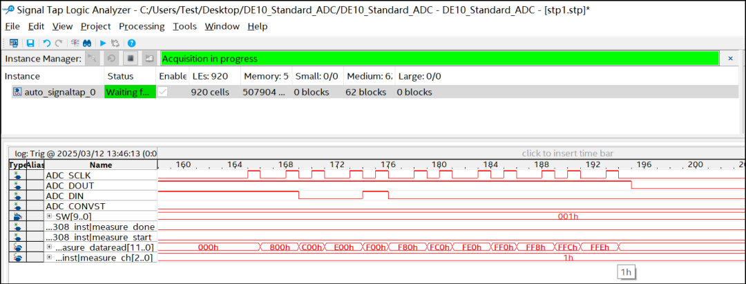
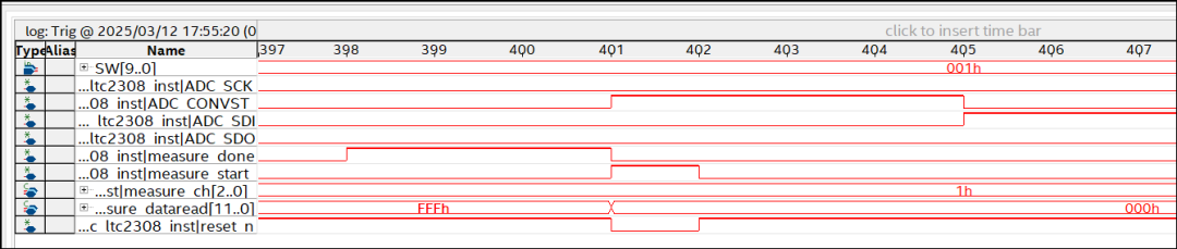
If the stp1.stp file sampling clock is set to 40M output from PLL outclk_1, the waveform details are as follows:
ADC_CONVST occupies 4 clock cycles (tick=0, 1, 2, 3):
Related Reading

01 – Design of a Digital Voltmeter Based on FPGA and LTC2308 (Overview)
02 – Design of a Digital Voltmeter Based on FPGA and LTC2308 – Principles of Analog-to-Digital Conversion
03 – Design of a Digital Voltmeter Based on FPGA and LTC2308 – Interpretation of the LTC2308 Datasheet
04 – Design of a Digital Voltmeter Based on FPGA and LTC2308 – Detailed Explanation of SPI Protocol
END