1
Introduction
The LTC2308 is a low-noise, 12-bit high-precision, successive approximation, 8-channel analog-to-digital converter (ADC) from Analog Devices Inc. (ADI), with a sampling rate of up to 500 kSPS (the maximum input signal frequency should not exceed 500 kHz; according to the Nyquist sampling theorem, it is recommended that the input signal be below 250 kHz), an SPI input clock of up to 40 MHz, and support for the Serial Peripheral Interface (SPI).
2
Functional Block Diagram and Pin Definition of LTC2308
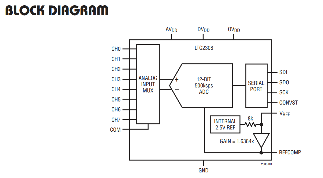
Functional block diagram of LTC2308:
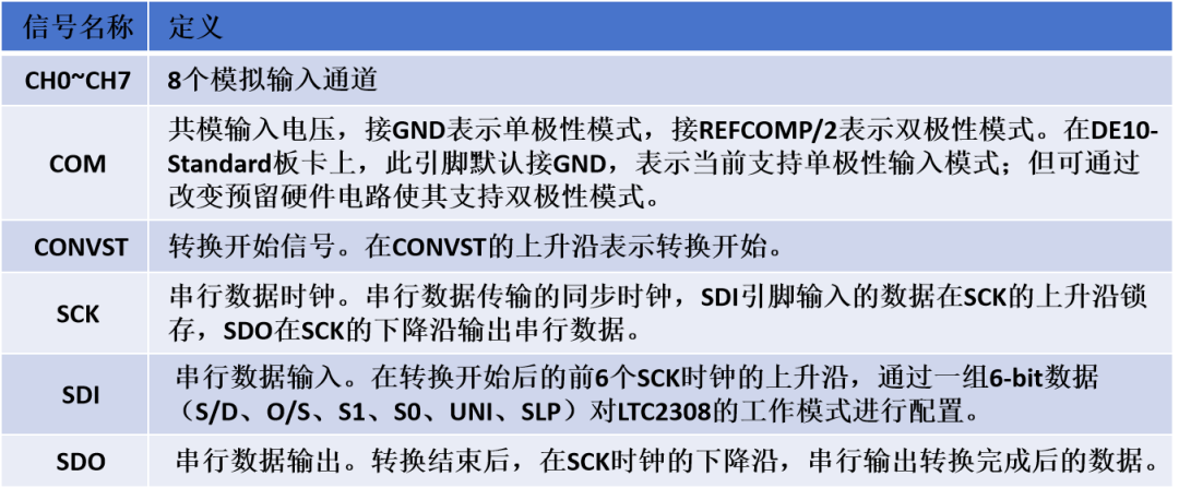
Pin definitions (refer to page 7 of the LTC2308 datasheet LTC2308fb.pdf):
3
Configuration of LTC2308 Operating Modes
The 8 analog channels of the LTC2308 can be configured as single-ended, differential channels, as well as unipolar and bipolar channels, connected via a four-wire SPI to other digital interface circuits.
In single-ended input mode, each channel can input a range of 0 to 4.096V in unipolar mode, and ±2.048V in bipolar mode, where negative values are represented in two’s complement form. In differential mode, CH0 and CH1, CH2 and CH3, CH4 and CH5, CH6 and CH7 can form differential pairs, allowing simultaneous sampling of differential signals to reduce common-mode interference. When the input source has a high impedance, the required signal acquisition time will also increase accordingly.
The various operating modes of the LTC2308 can be programmed using a 6-bit DIN word. (Refer to the timing diagram below, from page 10 of the LTC2308 datasheet LTC2308fb.pdf).
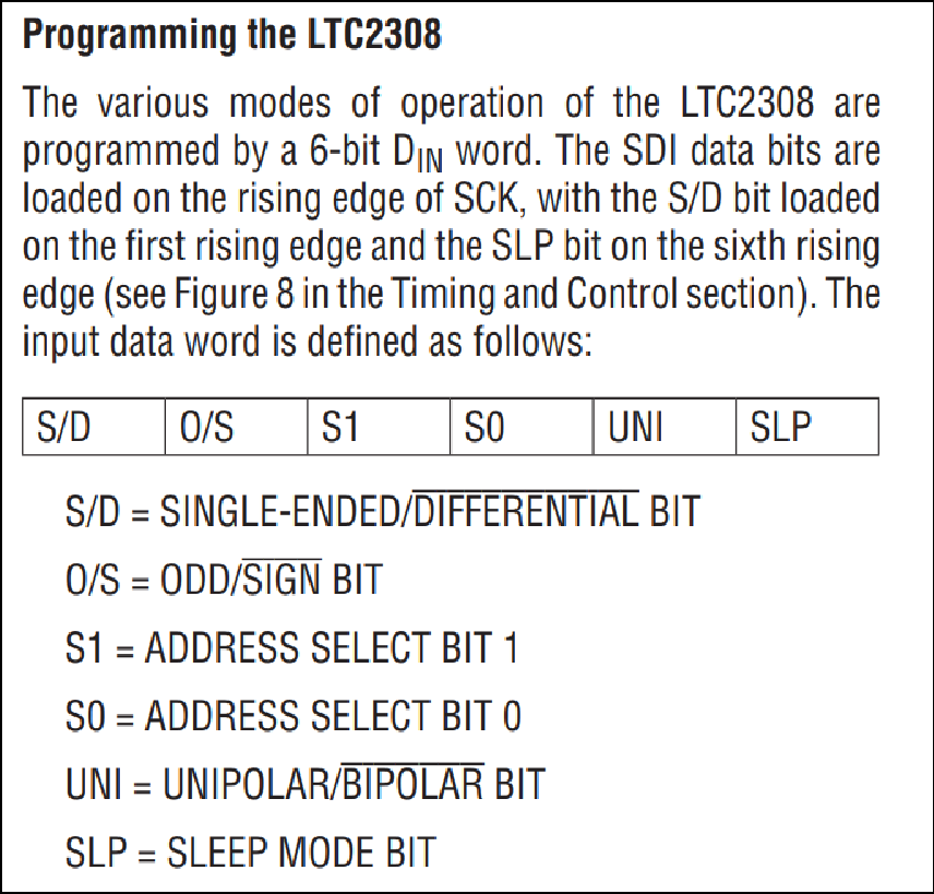
The definition of the 6-bit DIN word is as follows:
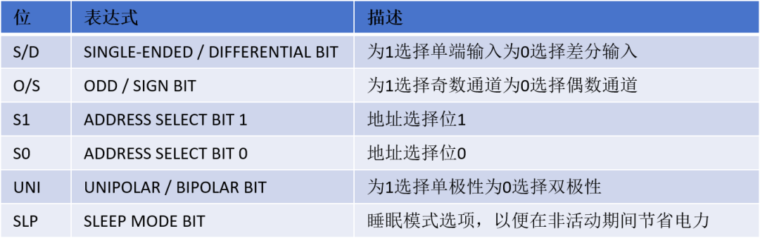
The control data for LTC is 6 bits, from high to low: S/D, O/S, S1, S0, UNI, SLP.
-
S/D controls whether the chip is in single-ended or differential mode.
-
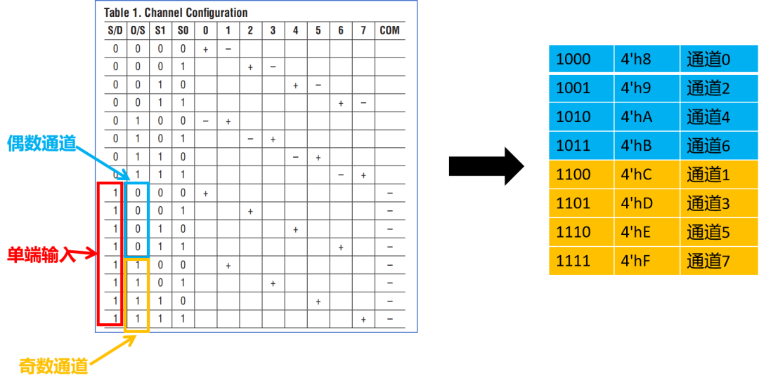
O/S controls the polarity of the two signals in differential mode; when O/S is 1, it indicates that the odd channel input signal is positive and the even channel input signal is negative; when O/S is 0, it indicates that the odd channel input signal is negative and the even channel input signal is positive. In single-ended mode, when O/S is 1, it indicates that the odd channel input signal is positive; when O/S is 0, it indicates that the even channel input signal is positive.
-
In differential mode, S1 and S0 form a 2-bit channel selection signal, which can select 4 pairs of differential channels. In single-ended mode, S1 and S0 form a 2-bit channel selection signal used to select 4 channels from the odd channels and 4 channels from the even channels.
-
UNI is the polarity control signal; when it is 1, it outputs a unipolar signal, and when it is 0, it outputs a bipolar signal in two’s complement form.
-
SLP controls whether the chip enters SLEEP or NAP state.
After transmitting the 6th control word, the chip requires at least 240 ns of tACQ acquisition time before CONVST can be pulled high again to initiate the next conversion.
Continuing to refer to Table 1 on page 10 of the LTC2308 datasheet LTC2308fb.pdf, we can obtain the configuration word for channel selection in this case:
4
Functional Block Diagram and Pin Definition of LTC2308
Refer to page 17 of LTC2308fb.pdf, there are two timing diagrams for the SPI protocol of this device.
The first:
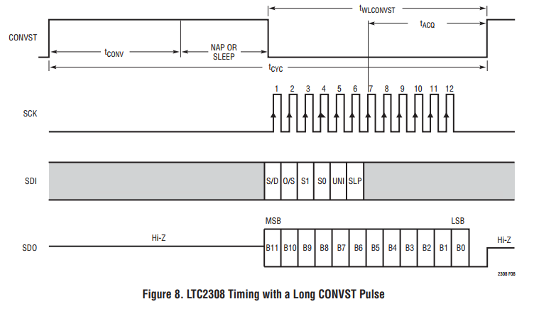
In the first timing diagram, when the conversion is complete, if CONVST remains high, the chip will enter NAP (SLP=0) or SLEEP (SLP=1) mode based on the logic level set by the SLP bit. When CONVST returns to low, the LTC2308 is released from SLEEP mode, requiring 200 ms to wake up and charge the 2.2uF capacitor on the VREF pin and the 10uF capacitor on the REFCOMP pin.
The second:
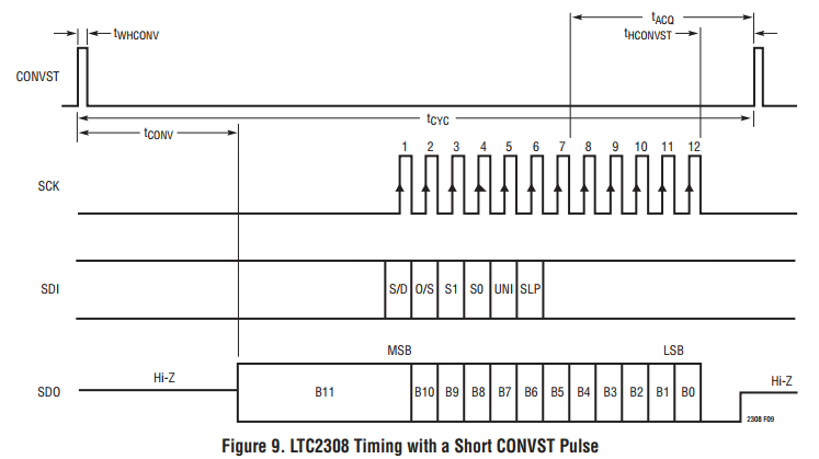
In the SystemCD\Demonstrations\FPGA\ADC case of DE10-Standard, we use the second timing diagram to achieve better performance of the LTC2308, aiming to:
1. Return to low level within 40 ns after the conversion starts
2. Return to low level after the conversion ends
For a description of this, please refer to page 14 of LTC2308fb.pdf:
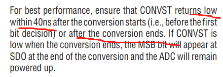
Therefore, the second timing diagram is chosen for the experiment.
The various time definitions in the second timing diagram (refer to page 5 of LTC2308fb.pdf):
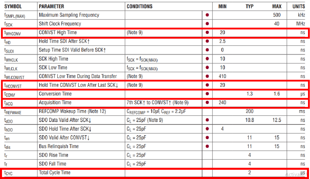
Extracting and translating the above table as follows:
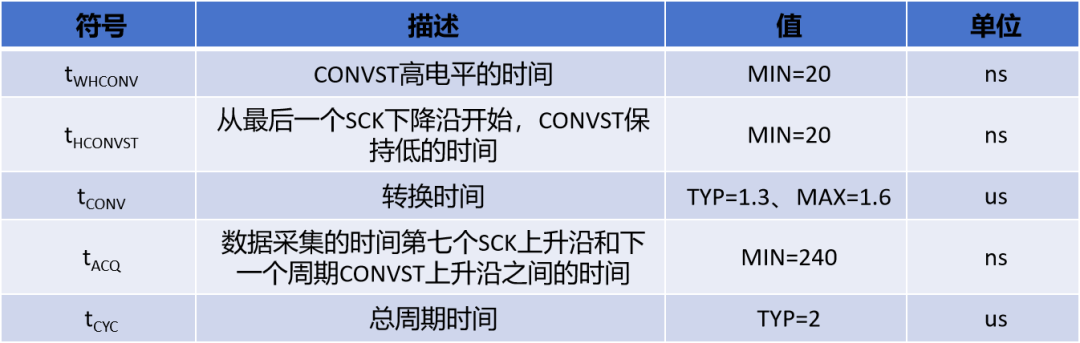
The second timing diagram shows that before the conversion time ends, the CONVST signal returns to low level. In this mode, the ADC and all internal circuits remain powered. After the conversion is complete, the MSB of the output data sequence from SDO will be valid after the data bus is enabled. After 1.3μs following the rising edge of CONVST, SDO will output data from the LTC2308 in rhythm with the SCK pulses, while SDI will load configuration data into the LTC2308. The first rising edge of SCK will load the S/D bit into the LTC2308, and the sixth rising edge of SCK will load the SLP bit into the LTC2308. SDO outputs data on the falling edge of each SCK pulse.
After sending the convert trigger, the SPI clock can only be sent after tCONV time, receiving the ADC result through SDO, and simultaneously setting the mode for the next convert through SDI. After the SPI clock ends, at least tHCONVST time must be waited before sending the next convert trigger. The LTC2308 is designed to start sampling after the control word is sent (the control word is sent after the 6th clock, and sampling can begin after the 7th clock) to accommodate the timing requirements under different modes.
Previous Readings

01 – Design of a Digital Voltmeter Based on FPGA and LTC2308 (Overview)
02 – Design of a Digital Voltmeter Based on FPGA and LTC2308 – Principles of Analog-to-Digital Conversion
END