Thanks to the rapid development of emerging industries such as 5G, big data, cloud computing, the Internet of Things, and artificial intelligence, the demand for memory has increased exponentially. At the same time, as application fields and usage scenarios become increasingly diverse, the market’s functional requirements for NAND Flash have also risen. To ensure its normal storage operation, precise and comprehensive testing has become even more important.
Advantages of NAND Flash Memory
As a type of non-volatile memory, NAND Flash memory is widely used in various electronic devices such as smartphones, digital cameras, and in-car navigation systems. The working principle of NAND Flash memory gives it many advantages. Firstly, it has fast read and write speeds, allowing devices to read and write data more quickly. Secondly, it has a high storage density, enabling it to hold more data in a relatively small size, making it an ideal choice for mobile devices and other embedded systems. Thirdly, its high reliability and low power consumption allow it to perform excellently in various application scenarios.
NAND Flash Memory Testing Solutions
To ensure that NAND Flash memory operates normally on electronic equipment, and to maintain the stability and reliability of its storage systems and data centers, comprehensive reliability testing is particularly important. The technical team at Xicai Component Screening Center has designed an MT29F64G08 NAND Flash memory adapter based on user requirements and the principles of device functionality and testing, which, when used with the T800C testing machine, can perform multiple verifications and tests.
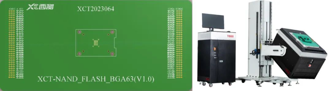
▲MT29F64G08 Adapter, T800C Testing Equipment
The T800C can provide 256 I/O channels, meeting the channel selection for NAND FLASH, with each channel supporting a maximum signal frequency of 400Mbps. It supports parameter testing for memory read, write, and erase currents at rates within 200MHz. Additionally, the T800C is equipped with an MTO module that can quickly traverse large-capacity storage chips for full-capacity testing and verification, replacing traditional methods that require manual data input for each memory or switching devices for capacity verification. The MTO module can also accurately locate memory bad blocks and capacity insufficiency issues. Therefore, using the T800C for memory testing results in shorter testing times and higher efficiency.
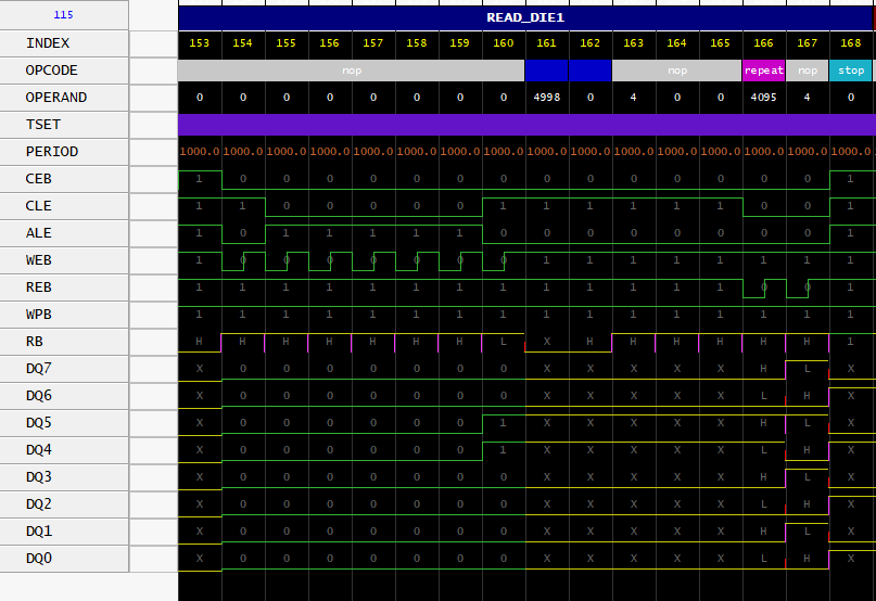
Function Verification
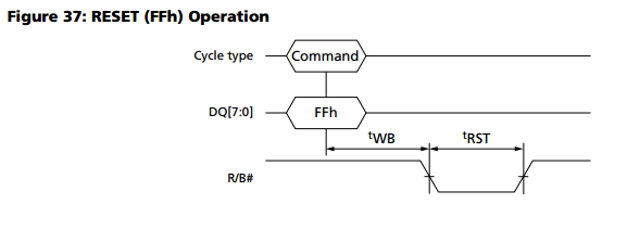
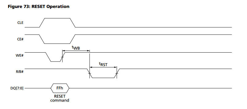
By performing a series of function verifications such as reading ID, reset, erase, programming, and reading, the internal timing and instructions of the chip are verified to comply with specifications.Reset (RESET Operation)Sets the target to its default power-on state and halts the ongoing command sequence, resetting all LUNs under that target.
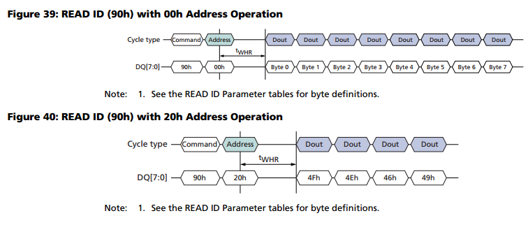
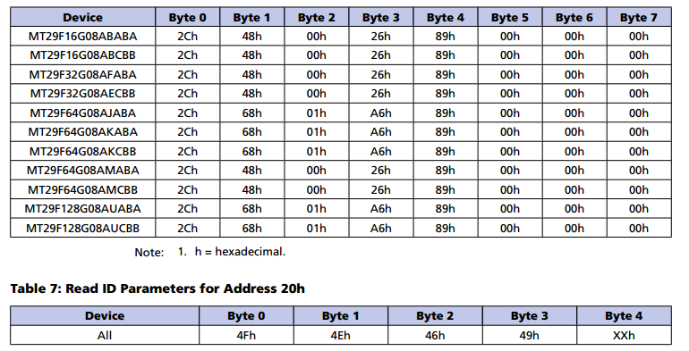
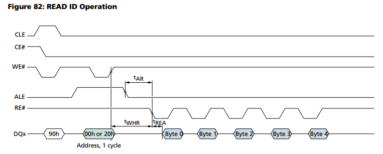
Read ID (READ ID)When the device is manufactured, different manufacturers will record some “identity” information on the chip according to different standards. We refer to this as the ID code, which can be read sequentially through chip instructions. If the read ID code matches the specifications in the device manual, the tested device can be considered the same model. The ID code typically contains manufacturer information, device capacity, and other details.
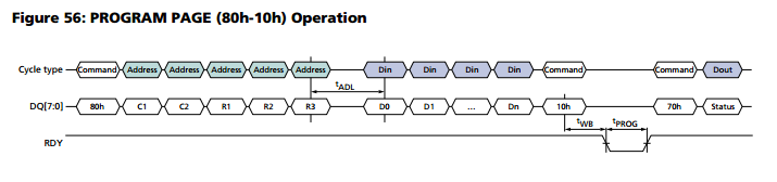
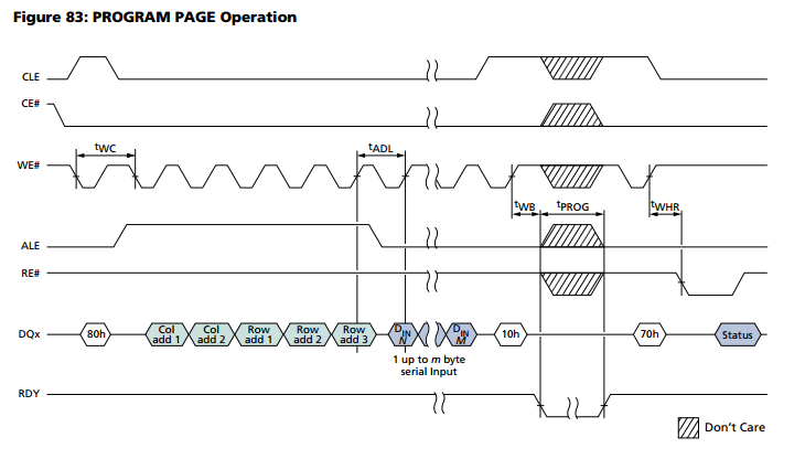
Page Programming (Page Program)After completing the write command operation, memory can be manipulated, typically using page programming, which allows writing 1 to 4096 bytes of data to memory in one page. After inputting the page programming command and selecting the starting address, programming data can be entered, and the chip will automatically increment the address based on the written data. Once the operation is complete, the R/B# pin will transition from low to high.
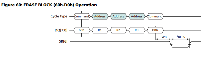
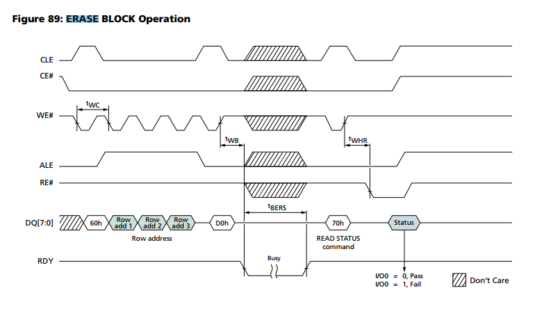
Sector Erase (Sector Erase)After completing the page erase command operation, input the starting address of the page to be erased. The Sector Erase selects the page erase operation, and once completed, the R/B# pin will transition from low to high.
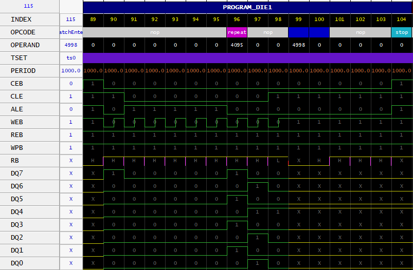
Test vectors can be located through the device’s vector editor tool to facilitate error checking and debugging.
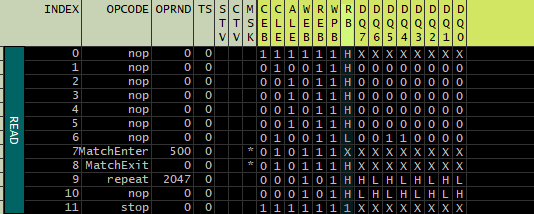
▲Test Vectors
Real-time waveforms can be captured using graphical tools to verify the stability and accuracy of system test results.
▲PROGRAM Test Waveform
▲READ Test Waveform
Combining device functionality to verify the ICC_Program, ICC_Read, ICC_Erase, VOH, VOL, ILI, ILO, and other DC characteristic parameters, the test results are accurate and stable, and the testing scheme comprehensively covers the device’s functionality and performance.
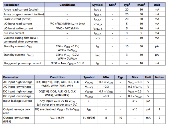
▲DC Parameter Table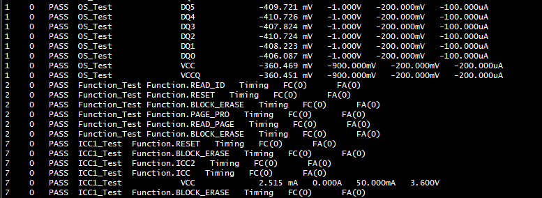 ▲Test Passed Data
Looking to the future, the Xicai Testing Component Screening Center will continue to summarize testing and screening experiences, adhering to the quality policy of being scientific, fair, practical, and surpassing, continuously enhancing the center’s innovation capabilities and service levels, and making breakthroughs in innovative research in the electronic field to provide more comprehensive technical support for the company’s electronic sector.
Previous Review
XCTT| About Us
Xian Xicai Testing Technology Co., Ltd. (Stock Code: 301306) was established in June 2010, headquartered in Xi’an. The company currently has three experimental parks located on Zhangba 2nd Road, Biyuan 2nd Road, and Xitai Road, covering a total area of over 30,000 square meters. It is currently the most comprehensive military third-party inspection and testing institution in the western region, with rich testing standards and a wide range of service fields. Xicai has built a one-stop testing technology service institution that integrates “technical support, inspection and testing, standard drafting, program consulting, and personnel training.”

Scan the QR code above to follow us