In the past two years, I have visited hundreds of companies and have recently spent time systematically organizing and summarizing information. In today’s electronic information field, the pace of cross-industry integration is accelerating, and the connections between various links in the industrial chain are tighter than ever. Therefore, when looking at a field or a project, it is necessary to consider the entire industrial chain comprehensively, including cloud management, hardware, software, algorithms, and data. Companies in each segment of the industrial chain are constantly integrating forward or backward, and competitive relationships can change at any time. With the advent of a new hardware era, research on the industry has raised higher requirements, and the dimensions of thinking need to broaden. It is essential to clarify the intricate relationships and future development trends, with the workload being several times greater than before. Research on benchmark companies in each segment of the industrial chain is a necessary task; only by understanding the strategies and movements of these large enterprises can one discover potential entrepreneurial/investment opportunities. Therefore, I have recently been consciously researching large enterprises, such as those in audio, visual, IoT platforms, and this article mainly focuses on ADAS chip manufacturers, to understand their main product lines and status.
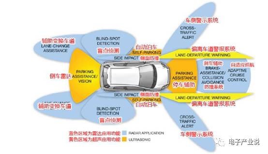
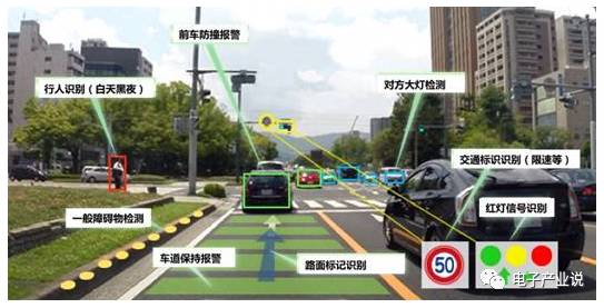
ADAS (Advanced Driver Assistance Systems) refers to the use of various sensors installed in vehicles to collect environmental data inside the vehicle in real-time, performing technical processing such as recognition, detection, and tracking of static and dynamic objects, thereby allowing drivers to detect potential dangers as quickly as possible. Typically, it includes navigation and real-time traffic systems (TMC), electronic police systems (ISA), adaptive cruise control (ACC), lane departure warning systems (LDWS), lane keeping systems, collision avoidance or pre-collision systems, night vision systems, adaptive lighting control, pedestrian protection systems, automatic parking systems, traffic sign recognition, blind spot detection, driver fatigue detection, downhill control systems, and electric vehicle alarm systems.
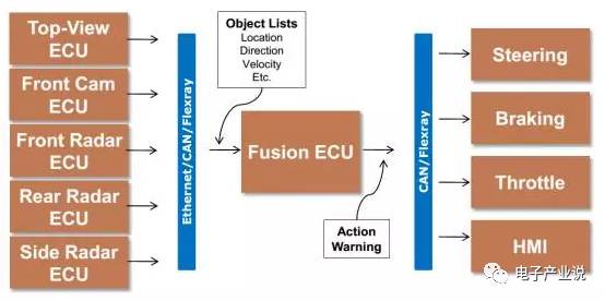
Currently, most innovations in automobiles come from innovations in automotive electronics. From the perspective of automotive electronic systems, they are gradually evolving from a distributed architecture (numerous ECUs controlling) to a centralized or even super control system (super processors). This trend is also reflected in ADAS. Changes in this trend include reducing ECUs, lowering power consumption, improving processor and memory utilization efficiency, reducing software development difficulty, and enhancing safety, making automotive semiconductor manufacturers play an increasingly important role in the entire automotive industry. At the same time, for ADAS processor chips, they currently exhibit product forms similar to smart home products, with single product hits and multifunctional combinations, such as Mobileye’s visual processing ADAS chip products and multi-sensor fusion, making ADAS chips trend towards becoming platforms. Currently, both forms have markets; single-function products will enable ADAS to be more widely adopted in mid-range and low-end vehicles, even in aftermarket markets, with cost-effectiveness being a prerequisite. Meanwhile, multi-sensor fusion will elevate the level of autonomous driving towards Level 4 or even Level 5. Currently, companies like Google and Baidu are working on multi-sensor fusion, but so far, there are no dedicated Level 4/5 ADAS ASIC chips.
From the perspective of chip design, the main challenges for ADAS processor chips currently lie in the following aspects:
1) Automotive-grade standards, preferably passing ISO26262, reaching ASIL-B or even ASIL-D levels.
2) High computational load and high bandwidth, especially for multi-sensor fusion chips, which require higher chip frequencies and heterogeneous designs to achieve fast data processing speeds, while also having high throughput requirements for data transmission.
3) With the application of artificial intelligence in ADAS, chip design will consider adding hardware for deep learning. How to make trade-offs between hardware and software, and how to match artificial intelligence computing models with existing hardware and software architectures and the entire system design is still in the early exploration stage.
Below, I will mainly introduce the products of major ADAS processor chip manufacturers, hoping to gain insight into the current state of the ADAS processor chip field and future development trends from their products.
Qualcomm/NXP
Since Qualcomm has acquired NXP, I will introduce them together here. Qualcomm is gradually entering the ADAS market mainly through its mobile processor chips (modified to automotive-grade). Initially, they started with surround view systems, and recently collaborated with Zongmu to launch the first ADAS product prototype based on the Snapdragon 820A platform and utilizing deep learning at CES. This product runs on the 820A neural network processing engine (SNPE), capable of recognizing various objects such as vehicles, pedestrians, and bicycles, as well as performing real-time semantic segmentation of drivable areas at the pixel level. However, it is still some distance from commercialization. Overall, Qualcomm’s Snapdragon product strategy should still focus on in-car entertainment information systems, gradually expanding into more specialized ADAS.
At the same time, NXP and the previously acquired Freescale have a complete product line layout in automotive electronics and ADAS chips.
NXP has released the Blubox platform, providing OEM manufacturers with a design, manufacturing, and sales solution for Level 4 (SAE) autonomous vehicles. The following diagram is the ADAS system block diagram from NXP, which fuses data from multiple video sources and 77G radar, then transmits it to the cloud and vehicle body systems. We see that NXP is a company capable of providing a complete set of reference solutions, with a comprehensive product line in this area. Although they have not integrated more chips, they provide relatively dispersed chips and solutions. Here, we will focus on the central processors S32V234 and MPC5775K. The MPC5775K processes radar data, while the S32V234 fuses and analyzes data processed from multiple sensors, transmitting the results to the vehicle body system via CAN bus.
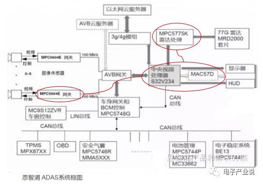
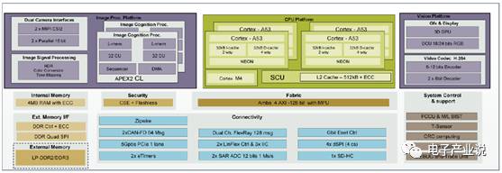
S32V234 is NXP’s ADAS processor launched in 2015 as part of the S32V series, supporting heterogeneous computing with CPU (4 ARM V8 architecture A53 and M4), GPU (GC3000), and image recognition processing (CogniVue APEX2 processors) with a low power design of 5W. Through CogniVue APEX2 processors, it can simultaneously support four automotive cameras (front, rear, left, right), extracting and classifying images, while the GPU can perform real-time 3D modeling, achieving a computational load of 50 GFLOPs. Therefore, based on this hardware architecture, it can complete 360-degree surround view and automatic parking functions. At the same time, this chip reserves interfaces to support millimeter-wave radar, laser radar, and ultrasonic sensors, facilitating multi-sensor fusion. This chip supports ISO 26262 ASIL B standards.
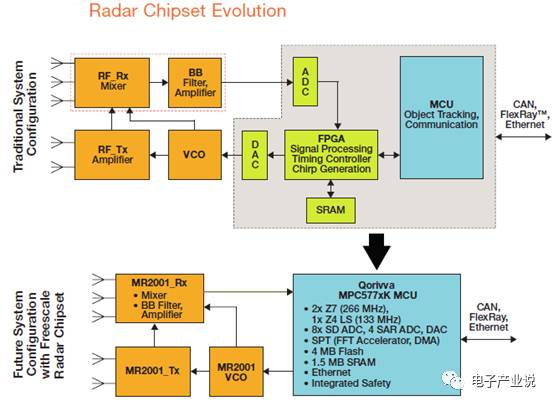
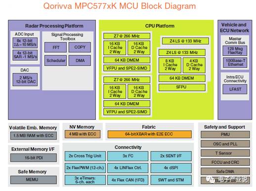
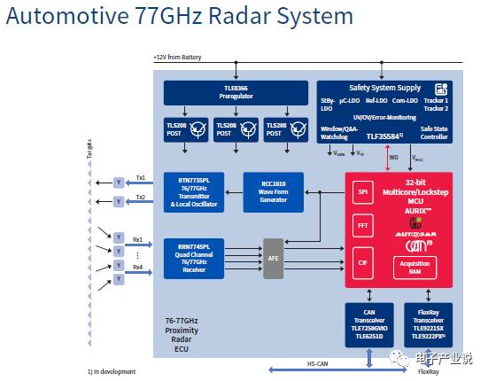
The Qorivva MPC567xK series is based on Power Architecture® 32-bit MCU, and the MPC577XK is a dedicated radar information processing chip. This series increases the chip’s memory, enhancing speed and performance, capable of supporting adaptive cruise control, intelligent headlight control, lane departure warning, and blind spot detection applications. From the perspective of the entire radar system, it combines the 77G radar transceiver chip set, Qorivva MPC567xK MCU, FPGA, ADC, DAC, and SRAM, supporting long, medium, and short-range applications. It is important to focus on the signal processing toolbox design, which includes FFT, DMA, COPY, and Scheduler. Currently, the 77GHz FCMW radar requires FFT, i.e., Fast Fourier Transform, in digital signal processing, with typical sampling points for automotive radar ranging from 512 to 2048. From the chip architecture diagram, we see a dedicated FFT circuit.
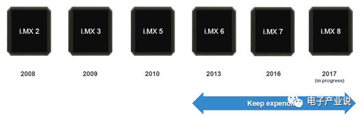
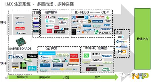
In addition to the S32V series, the acquired Freescale has a well-known i.MX series chip that can also serve as a central processor. The i.MX series, especially the i.MX6, has extensive applications in automotive, particularly in in-car information systems. Many automotive manufacturers use i.MX.
Intel/Mobileye/Altera
Through a series of acquisitions, Intel has completed its layout in ADAS processors, including Mobileye’s ADAS visual processing, utilizing Altera’s FPGA processing, and Intel’s own Xeon and other processor models, forming a complete hardware super central control solution for autonomous driving.
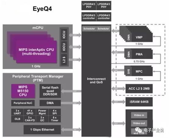
It is particularly noteworthy that Mobileye’s EyeQ series has been adopted by many automotive manufacturers, including Audi, BMW, Fiat, Ford, General Motors, Honda, Nissan, Peugeot, Citroën, Renault, Volvo, and Tesla. The recent EyeQ4 has demonstrated performance reaching 25 trillion operations per second, with a power consumption as low as 3W. From the hardware architecture perspective, this chip includes a set of industrial-grade quad-core MIPS processors operating at 1GHz, supporting innovative multithreading technology for better data control and management. Multiple dedicated vector microcode processors (VMP) are used to handle ADAS-related image processing tasks (such as scaling and preprocessing, warping, tracking, lane marking detection, road geometry detection, filtering, and histogramming). A military-grade MIPS Warrior CPU is located in the secondary transmission management center to process both internal and external general data.
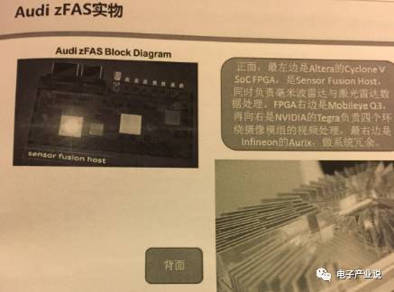
Currently, the fusion mainly involves radar and camera integration, which requires bandwidth that general ASICs can meet. However, for integrating LiDAR, it is best to use FPGA, as FPGA is the most suitable for sensor hubs. At the same time, sensor fusion is currently applied less frequently, and suitable ASICs are hard to find, making FPGA the mainstream choice. Additionally, for some high-precision radars, such as using single-precision floating-point processing to implement a 4096-point FFT, the more sampling points, the smaller the error, but the computational load will increase significantly. It inputs and outputs four complex samples per clock cycle. Each FFT core runs at speeds exceeding 80 GFLOPs, which generally requires FPGA for better implementation. Typically, automotive radar sampling points range from 512 to 2048, but military applications can reach 8192, necessitating FPGA support. As shown in the physical example of AudizFAS, an Altera Cyclone V SoC FPGA is used for sensor fusion, also responsible for processing millimeter-wave radar and LiDAR data.
Renesas
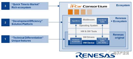
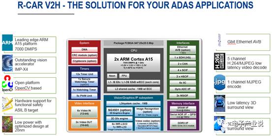
Renesas provides a relatively complete product line for ADAS processors and also offers ADAS Kit development systems. Among the chip series, the most famous is its R-Car product line, which includes high-end products with hardware architectures comprising ARM Cortex A57/53, ARM Cortex R series, Video Codec, 2D/3D GPU, ISP, etc., capable of supporting multiple visual sensor inputs and compatible with software such as OPENGL and OpenCV, meeting ASIL B automotive-grade standards. In fact, this product was initially used for in-car infotainment systems, and later the system products gradually adapted to automotive surround vision systems, dashboards, and ADAS systems. This development path is worth referencing for domestic semiconductor manufacturers looking to enter the automotive field.
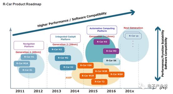
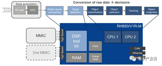
In addition to the R-Car series products, like NXP, Renesas also has specialized processing chips for radar sensors such as the RH850/V1R-M series, which adopts 40nm embedded eFlash technology, and optimized DSP for fast FFT processing.
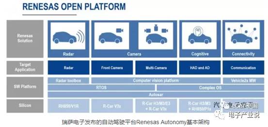
Recently, it has been reported that Renesas launched Renesas Autonomy, a newly designed ADAS and autonomous driving platform. Specific details are still unclear, but according to Amrit Vivekanand, Vice President of Automotive Business at Renesas Electronics America, the newly launched autonomous driving platform is different from competitors, “This is an open platform, hoping to make it easier for users to port their algorithms, function libraries, and real-time operating systems (RTOS) onto the platform.” The first product released on the Renesas Autonomy platform is an image recognition system-on-chip (SoC) called R-Car V3M. Renesas describes this high-performance visual processing chip as an “optimized processing unit, primarily applied to smart camera sensors, but can also be used for surround vision systems and even LiDAR data processing.” According to Mike Demler, a senior analyst at semiconductor industry analysis firm Linley Group, the release of this open platform and product can be seen as Renesas’s positioning against Mobileye, “They hope to attract automotive manufacturers that have not partnered with Mobileye, especially Japanese manufacturers, and also hope to attract some Tier 1 manufacturers producing ADAS products.” Compared to Mobileye’s processing platform, which is a “black box” system, Renesas emphasizes the “openness” of its solutions, which is a topic that every processor manufacturer aiming to compete with Mobileye tends to discuss. Renesas has stated that all algorithms of its latest R-Car V3M processing module will be open to its users.
Infineon
As a global market leader in automotive electronics, power semiconductors, and smart card chips, Infineon has long provided semiconductor and system solutions for automotive and other industrial applications. Infineon has leading technology in 24/77/79G radar, LiDAR, and other sensor devices and processing chips. In addition, they have their own solutions in body control, airbags, EPS, TPMS, and more.
Texas Instruments (TI)
TI actually has two product lines in ADAS processors, the Jacinto and TDA series. The Jacinto series is mainly developed based on the previous OMAP processors. After TI abandoned the mobile processor platform, it focused its digital processors on automotive applications, mainly in-car infotainment systems. However, from Jacinto6, we see the combination of in-car infotainment and ADAS functions. This chip includes dual ARM Cortex-A15 cores, two ARM M4 cores, two C66x floating-point DSPs, multiple 3D/2D graphics processors (Imagination), and also integrates two EVE accelerators. This Jacinto6 SoC processor is exceptionally powerful, whether in processing entertainment media or assisting driving with in-car cameras, it can utilize both internal and external cameras to present various functions such as object and pedestrian detection, enhanced reality navigation, and driver identification.
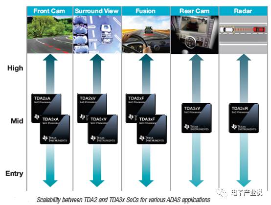
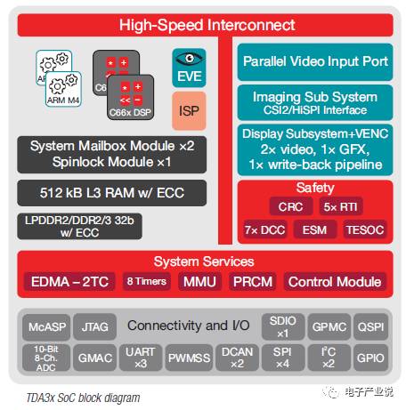
The TDA series has always focused on ADAS functions. The TDA3x series supports various ADAS algorithms such as lane line assistance, adaptive cruise control, traffic sign recognition, pedestrian and object detection, forward collision warning, and reverse collision warning. These algorithms are crucial for the effective use of front cameras, full vehicle surround view, fusion, radar, and intelligent rear cameras in numerous ADAS applications.
NVIDIA
With the rise of artificial intelligence and autonomous driving technology, NVIDIA’s GPUs, with their strong parallel computing capabilities, are particularly suitable for deep learning. It is generally believed that compared to Mobileye, which focuses solely on visual processing, NVIDIA’s solution emphasizes the fusion of different sensors. It is rumored that Tesla has abandoned Mobileye and adopted NVIDIA.
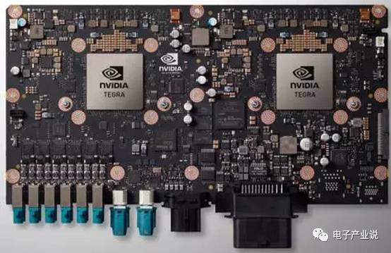
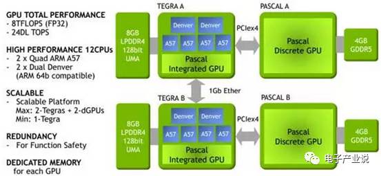
NVIDIA’s Drive PX2 is referred to by Jensen Huang as “the supercomputer designed for cars” and is set to become standard equipment in vehicles, capable of perceiving the car’s location, identifying surrounding objects, and calculating the safest path in real-time. “The Tegra X1 processor and 10GB of memory can simultaneously process images from 12 2-megapixel cameras at 60 frames per second, and through environmental visual computing technology and powerful deep neural networks, actively recognize various vehicles on the road, even detecting if a vehicle in front is opening a door. The Driver PX2 also incorporates chips from other partners, including Avago’s PEX8724 (24-lane, 6-port, third-generation PCIe Gen switch) for interconnection between two Parkers. There is also an FPGA provided by Altera, acquired by Intel, for executing real-time operating systems. The FPGA model is Cyclone V 5SCXC6, which is Altera’s top product, with logic operations of 110K and registers reaching 166036. Finally, there is an Infineon AURIX TC 297 MCU for safety control, reportedly allowing PX2 to reach ASIL C level. Additionally, there is Broadcom’s BCM89811 low-power physical layer transceiver (PHY), using BroadR-Reach automotive Ethernet technology, achieving transmission rates of up to 100Mbps over a single pair of unshielded twisted pairs. Therefore, NVIDIA has effectively launched a board-level ADAS system.
ADI
Compared to the aforementioned chip companies, ADI’s strategy in ADAS chips emphasizes cost-effectiveness. Currently, ADAS technology is primarily applied in high-end models due to high overall costs. ADI targets high, mid, and low-end vehicles, selectively launching certain ADAS technologies to achieve costs as low as $2 or a few tens of dollars, which is undoubtedly great news for vehicle manufacturers and consumers.
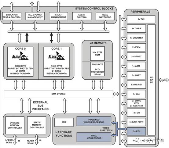
In visual ADAS, ADI’s Blackfin series processors are widely adopted, with low-end systems based on BF592 achieving LDW functionality; mid-range systems based on BF53x/BF54x/BF561 achieving LDW/HBLB/TSR functionalities; and high-end systems based on BF60x utilizing a “pipelined visual processor (PVP)” to achieve LDW/HBLB/TSR/FCW/PD functionalities. The integrated visual preprocessor can significantly reduce the burden on the processor, thereby lowering performance requirements on the processor.
It is worth mentioning that ADI recently launched Drive360TM 28nm CMOS RADAR technology (77/79GHz)
, which applies excellent RF performance to target recognition and classification, revolutionizing sensor performance in ADAS applications. ADI’s high-performance RADAR solutions can detect rapidly moving small objects in advance, while extremely low phase noise allows for the clearest detection of small objects in the presence of large objects. ADI has collaborated with Renesas to jointly launch a systematic solution for this chip, combining ADI’s RADAR with Renesas Autonomy platform’s RH850/V1R-M microcontroller (MCU).
Fujitsu
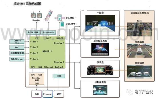
Fujitsu’s ADAS technology mainly involves the combination of cameras and sensors to achieve image recognition assistance and target detection. The application areas mainly include 360-degree 3D panoramic assistance, visual parking assistance, monitoring blind spots while driving, safely opening doors, and recognizing obstacles and pedestrians around the vehicle. This includes a panoramic video system based on the MB86R11 “Emerald-L” 2D/3D image SoC, supporting real-time panoramic video monitoring of the vehicle’s surrounding environment using four cameras (front, rear, left, right). Public information indicates that Fujitsu seems more keen on constructing virtual dashboards and in-car infotainment systems, but this area is the easiest for domestic chip companies to imitate and surpass.
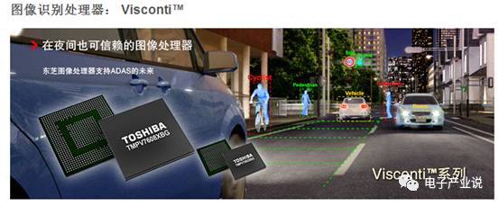
Toshiba
The latest news is that Toshiba will split its business into four parts: social infrastructure business, thermal power generation and other energy businesses, semiconductor and storage businesses excluding memory, and information communication technology (ICT) solutions business. Therefore, Toshiba has a lot of uncertainty in the future, but from the perspective of ADAS processors, Toshiba has image recognition processors in the Visconti series. Currently, the second-generation product (Visconti2) has been mass-produced and started to be deployed in mass production vehicles like the Toyota Prius through products from Denso since November 2015, with global shipments exceeding 30,000 units per month.
Visconti adopts a multi-core heterogeneous dedicated processor, and Visconti2 can process in real-time and parallel implement four functions, such as lane keeping, front vehicle detection, pedestrian recognition, and traffic sign recognition. The Visconti4 image recognition processor can easily recognize vehicles and pedestrians, as well as identify traffic signals, obstacles, and lane markings, enabling various advanced driver assistance applications such as lane departure warning, forward/reverse collision warning, and pedestrian collision warning, capable of processing and implementing eight functions simultaneously.
Xilinx
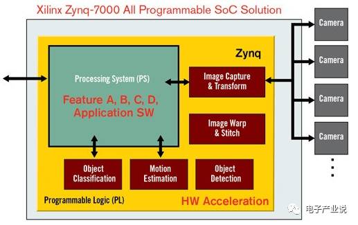
Xilinx is a well-known FPGA company whose products are widely used in various fields. The benefits of FPGA include programmability and flexible configuration, while also improving overall system performance, significantly shortening the entire development cycle compared to developing chips individually. However, the drawbacks include factors such as price and size. In automotive ADAS, Xilinx’s most widely used product is the Zynq®-7000 All Programmable SoC. This system (SoC) platform helps system manufacturers accelerate development time in applications such as surround vision, 3D surround vision, rearview cameras, dynamic calibration, pedestrian detection, rear lane departure warning, and blind spot detection. Zynq allows for the development of ADAS solutions using a single chip. The Zynq-7000 All Programmable SoC significantly enhances performance, facilitating various bundled applications and enabling scalability between different product lines. Furthermore, it provides an optimized platform for ADAS, allowing automotive manufacturers and automotive electronics suppliers to add their own IP and ready-made IP provided by the Xilinx automotive ecosystem to create unique differentiated systems.
This public account publishes original articles on industrial research in the electronic information field and discusses the path of industrial development with relevant individuals. You can also add the author’s WeChat account by scanning (please indicate: from the electronic industry discussion).