How Chips Are Made: From Ordinary Rock to Essential Technology
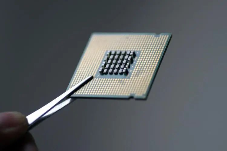
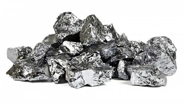
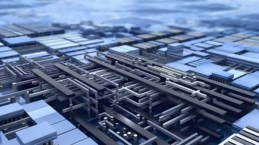
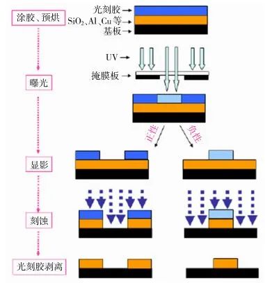
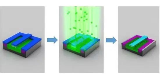
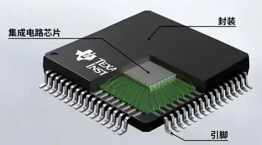
Click the above “Mechanical Electronic Engineering Technology” to follow usHey, friends! Are you curious about that mysterious thing in your phone and computer—the chip? Today, let me take you into this mysterious world and tell you how a chip transforms from an ordinary rock into the indispensable “golden finger” in our hands!Imagine, what would our world be like without chips? Phones can’t stream videos or play games, computers can’t work or browse the internet, and even the little smart speaker at home can’t chat with you. Chips, this seemingly insignificant little thing, carry the soul of our entire information age. So, how are they manufactured?1. The “Raw Materials” of ChipsFirst, we need to know that chips do not just fall from the sky, nor are they magically created. Their raw material is actually a type of rock called silicon. Yes, it’s rock! However, this silicon rock is not ordinary; it requires extremely high purity and must undergo multiple refinements and processes to become the basic material for chip manufacturing.2. Designing the Circuit DiagramWith the raw materials ready, the next step is to design the circuit diagram. This process is like drawing the design of a house on a piece of paper. Designers will draw complex circuit diagrams based on the functional requirements of the chip, including various electronic components and their connections. These circuit diagrams will be converted into a special file format for manufacturing equipment to use.3. Photolithography and EtchingNext comes the photolithography and etching phase. This process is like drawing a pattern on paper with a pencil and eraser. The manufacturing equipment first coats a silicon wafer with a special photoresist, then uses a light source to project the circuit diagram onto the wafer. This way, the photoresist gets exposed, forming a pattern corresponding to the circuit diagram.Then comes the etching. Etching is like using an eraser to remove the unnecessary parts. The manufacturing equipment uses chemical solutions or gases to etch away the areas not covered by the photoresist, leaving grooves and bumps corresponding to the circuit diagram. Thus, we obtain a preliminary shape of the chip.4. Doping and MetallizationHowever, this preliminary chip cannot be used directly. It still needs to undergo doping and metallization steps. Doping is like adding some “seasoning” to the chip; by introducing different impurity elements into the wafer, we change its conductivity to form electronic components with different functions.Metallization is like dressing the chip in “clothes”; a layer of metallic film is deposited on the wafer, and through photolithography and etching steps, the metallic film is cut into lines corresponding to the circuit diagram. These lines act like the blood vessels and nerves within the chip, responsible for transmitting signals and energy.5. Packaging and TestingThe final step is packaging and testing. Packaging is like putting a “shell” on the chip to protect it from external environmental influences. Testing checks whether the chip functions normally and whether its performance is stable. Only chips that pass strict testing can be delivered to us, becoming an indispensable part of our daily lives.6. Cutting-edge Technologies in Chip ManufacturingMany cutting-edge technologies are also applied in the chip manufacturing process. These technologies not only improve chip performance and quality but also reduce manufacturing costs and time.For instance, nanotechnology allows us to precisely control and manipulate materials at the nanoscale, creating smaller and more refined circuit structures and components. Additionally, 3D printing technology can directly print materials according to the circuit diagram in one go, greatly increasing manufacturing efficiency.Furthermore, automation and intelligent technologies are applied. By introducing advanced technologies like robotics and machine vision, automated operations can be achieved in wafer preparation, circuit design, photolithography, etching, and other processes. At the same time, techniques like big data and machine learning can be used for intelligent monitoring and optimization of the manufacturing process, enhancing product quality and production efficiency.You might wonder, with such complexity in chip manufacturing, it must take many years to complete, right? Actually, that’s not the case. With technological advancements and process improvements, the time required to manufacture a chip has been greatly reduced. From design to production, and then to packaging and testing, the entire process may only take a few months or even weeks.Moreover, did you know? Each chip is unique. Just like our fingerprints, every chip has its own number and serial number. This is because during the manufacturing process, every chip undergoes strict inspection and screening to ensure their functions and performances meet standards.Alright, having said all that, I believe you now have a general understanding of chip manufacturing, right? Chips may be small, but the technology and processes behind them are very complex. It is the continuous progress and innovation of these technologies and processes that have given us today’s intelligent and convenient information age.So, the next time you pick up your phone or open your computer, take a moment to think about that tiny chip! It acts like a little magician, lighting up our digital lives with its magic. Behind all this are the hard work and wisdom of countless scientists and engineers. Let’s give them a thumbs up together!