
1.
Learn the basics of chip architecture – a deep understanding is key;
2.
Learn the basics of chip manufacturing – materials, wafer preparation, patterning, and packaging;
3.
Start electronic design automation by building CMOS transistors layer by layer;
4.
Create my first complete circuit using Verilog – “My first experience programming hardware with software.”;
5.
Implement simulation and formal verification for my circuit;
6.
Design my first complete chip layout – using OpenLane (an open-source EDA tool) for design and optimization;
Initial Plan Formulated
1.
Start Preparing
-
Review circuit physics – (semiconductors, p-n junctions, diodes, capacitors) -
Review computer systems – (transistors, gates, combinational logic, sequential logic, memory, ALU, CPU, and von Neumann architecture, machine language, assembly, C)
2.
Chip Manufacturing – How are chips actually made?
-
Read “Microchip Fabrication” by Peter Van Zant, a popular science book on semiconductor processing and manufacturing -
Test: Rewatch @szeloof’s chip manufacturing video; everything should make sense and should be able to explain it
-
Understand the development of ASML machines -
Deep dive into how EUV works
3.
Architecture – What are the main chip designs used in today’s chips?
-
Understand x86 vs ARM vs RISC-V -
Deep dive into RISC-V (the chip tape-out will use RISC-V CPU)
4.
Electronic Design Automation –
How do you design and verify your own chip to be sent for manufacturing?
-
Learn from a blogger’s course on designing chips from scratch (learning chip design, verification, etc.) -
Design and test my own RISC-V ASIC using Verilog/OpenLANE/Caravel – I am currently considering making a minimal GPU or converter accelerator, but I am open to any ideas -
Submit chip designs to TinyTapeout
5.
ASIC – What specific application chips are used in different industries?
How do they work?
-
AI Accelerators – Untether, Tenstorrent, Etched, Groq -
Telecommunications – Network switches, routers, network cards, etc. -
Automotive – Engine Control Units (ECUs), Advanced Driver-Assistance Systems (ADAS), etc. -
Finance – FPGAs for high-frequency trading
6.
Technological Advances – How has technology progressed in the chip industry over the past decades?
-
Advancements leading to Moore’s Law -
Advancements in NVIDIA GPUs -
Progress in TSMC manufacturing processes
7.
Industry and Commerce – What are the dominant forces shaping today’s chip industry?
-
Read “Chip War” -
Understand the CHIPS Act and geopolitics -
Learn about the business of each stage of the chip industry value chain (IP cores, EDA, fab equipment, fabless chip companies, integrated device manufacturers, foundries, OSAT)
8.
Opportunities – What are the major opportunities in this field?
-
What major opportunities do large companies have? -
What important opportunity areas are suitable for young entrepreneurs? -
Where will venture capital bets be placed? -
Which companies are still good investments?
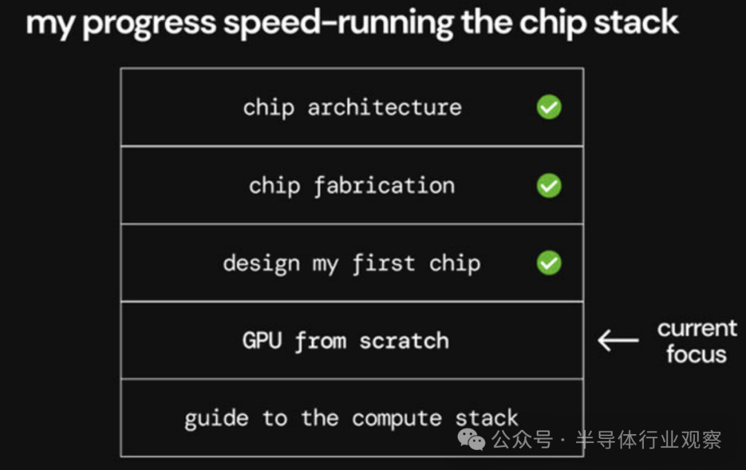
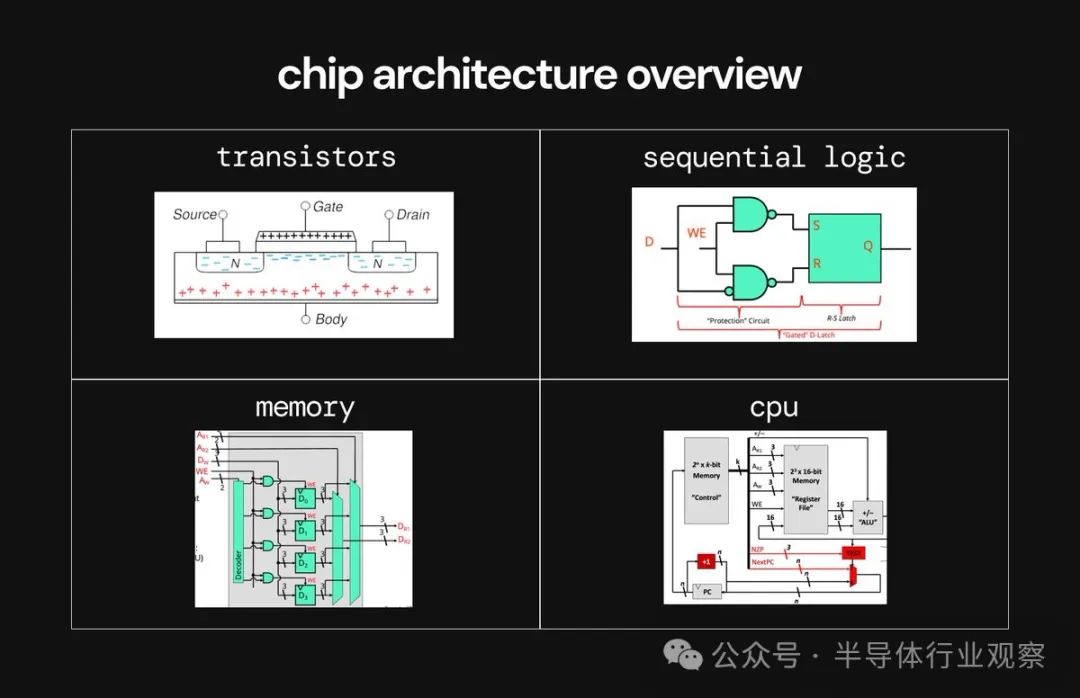
Step One: Learn the Basics of Chip Architecture
-
Binary – Encoding data using voltage -
Transistors – Creating digital switches using semiconductors -
CMOS – Building the first energy-efficient inverter using transistors -
Gates – Computing higher-level Boolean logic using transistors -
Combinational Logic – Building Boolean logic circuits using gates -
Sequential Logic – Persisting data using combinational logic -
Memory – Creating storage systems for data using sequential logic -
CPU – Combining memory and combinational logic to create the von Neumann architecture, which is the first step towards Turing completeness (ignoring memory constraints) -
Machine Language – How instructions in memory map to control signals on the CPU -
Assembly – How assembly maps directly to the CPU -
C – How C compiles to assembly language and then to machine language
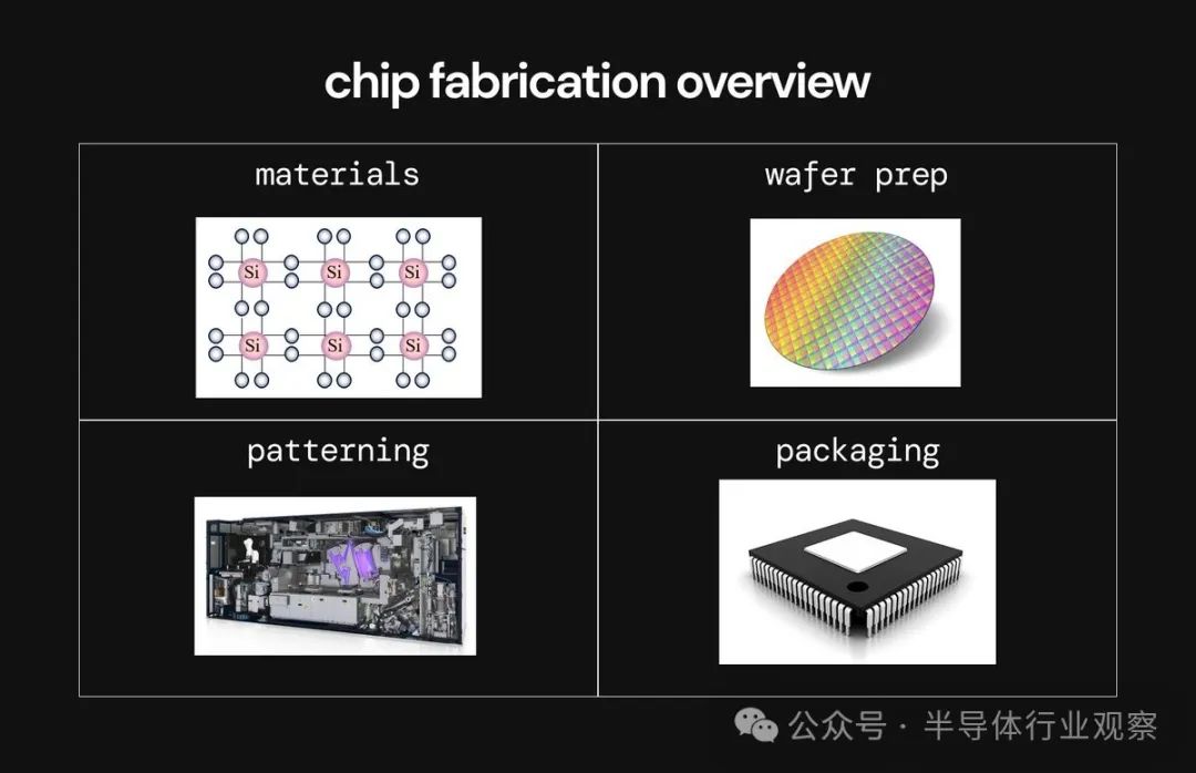
Step Two: Learn the Basics of Chip Manufacturing
-
Materials – Semiconductor manufacturing requires a lot of materials, including semiconductors, etchants, solvents, etc., each with specific qualities that are worth using. -
Wafer Preparation – Manufacturing silicon wafers with polycrystalline silicon crystals and “growing” a silicon dioxide layer on them -
Patterning – Creating the actual transistor patterns on the chip using a 10-step process involving layering (oxidation/deposition/metalization), photolithography, and etching -
Packaging – Encapsulating the chip in a protective cover to prevent damage, create I/O interfaces, assist with heat dissipation, etc. -
Contamination – Interestingly, as transistor sizes shrink, the focus on contamination control becomes significantly greater/important
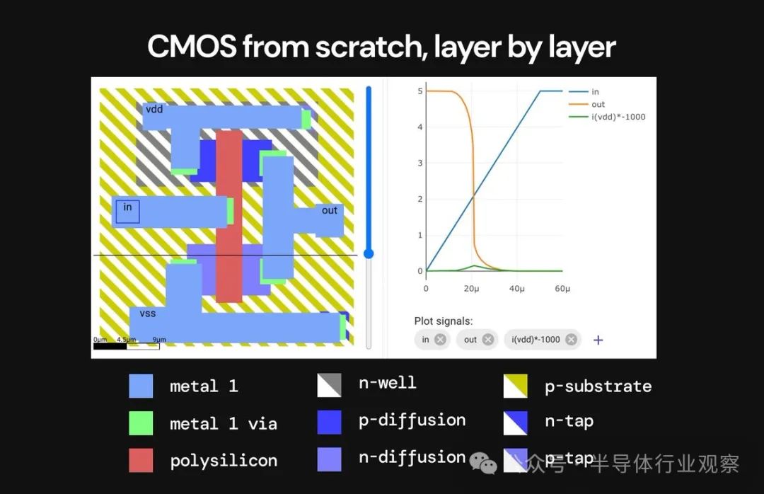
Step Three: Start Electronic Design Automation by Building CMOS Transistors Layer by Layer
CMOS transistors are the fundamental structure that allowed digital computing to take off due to their unique energy efficiency
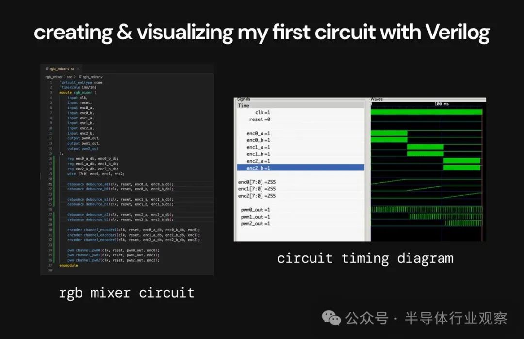
Step Four: Create My First Complete Circuit in Verilog
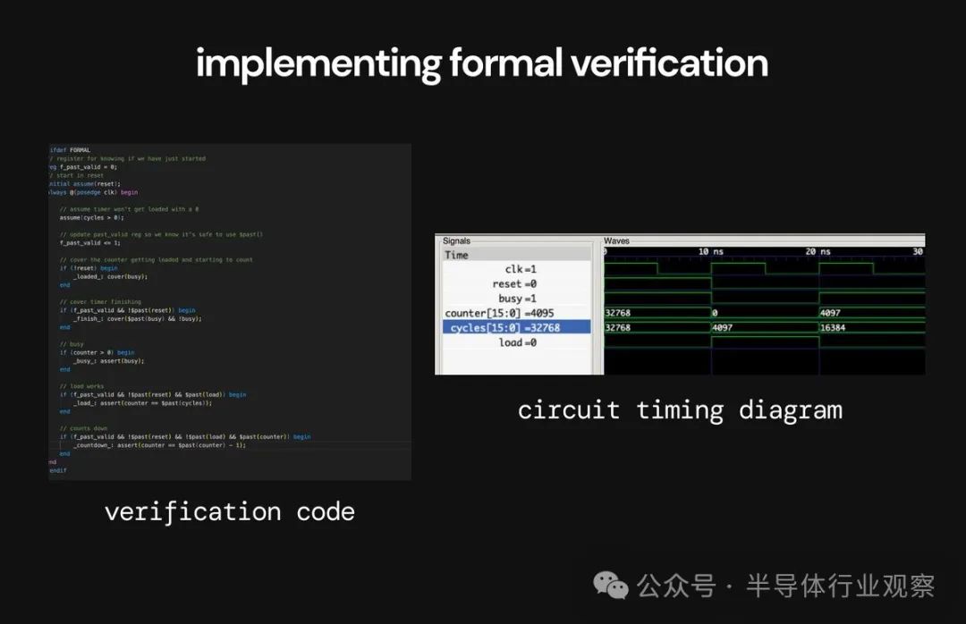
Step Five: Implement Simulation and Formal Verification for the Circuit
-
Static Timing Analysis – Ensuring there are no timing errors caused by signals propagating through the circuit; -
Bounded Model Checking and k-Induction – Ensuring your design cannot enter certain invalid states -
You also need to ensure the circuit can enter specific valid states
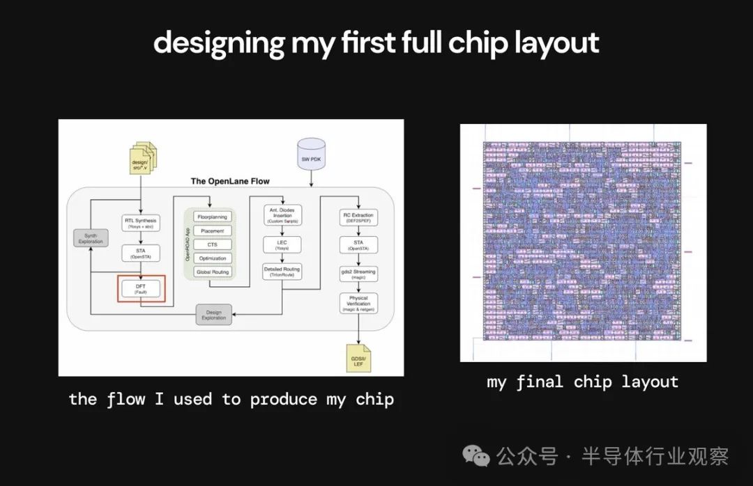
Step Six: Design My First Complete Chip Layout
-
Simulation – Running simulations to verify your design passes all test cases -
Synthesis – Converting HDL into a netlist that shows the connections between all the gates in the design -
Optimization – Optimizing the design for area, performance, and power consumption -
Layout – Arranging all standard cells on the physical chip -
Wiring – Connecting all components together through proper wiring -
Verification – Performing formal verification on the final design -
GDS – Creating the final output file, called a GDS2 file, to specify the exact layers to be sent to the foundry for tape-out
-
I can zoom in and view individual cells and transistors -
I can selectively hide different metal layers to understand how everything is connected -
I can view energy density, component density, etc., in my design
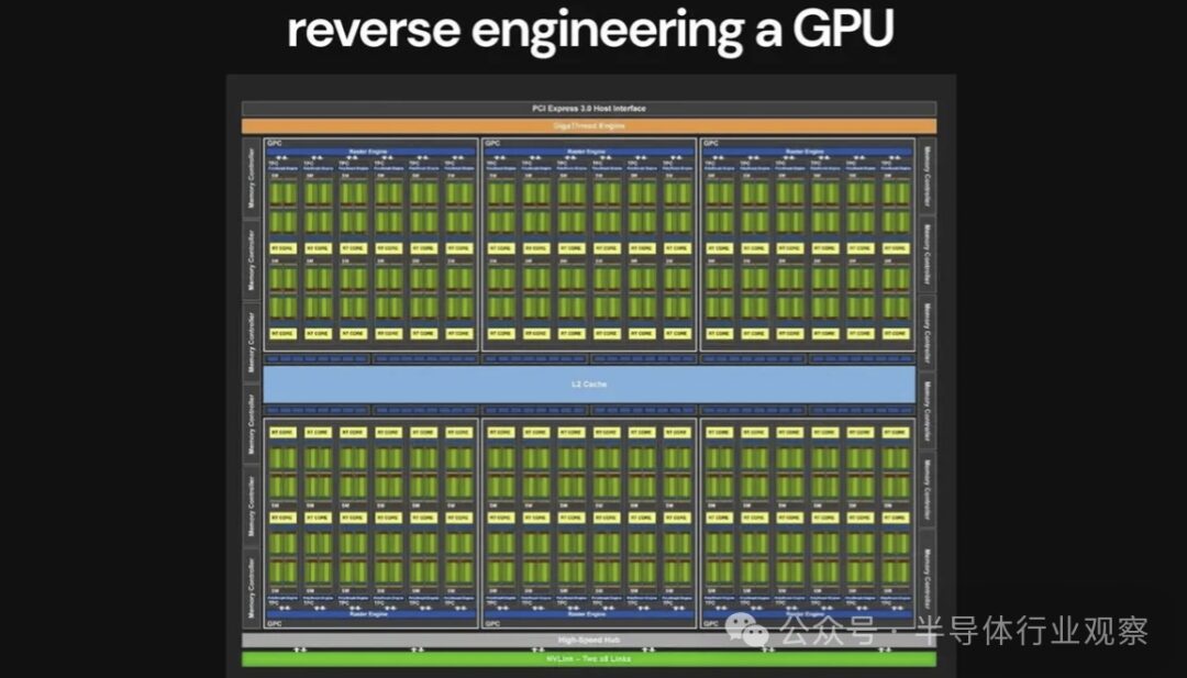
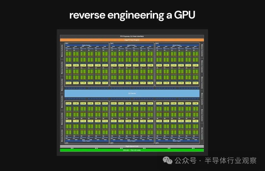
Step Seven: Reverse Engineer and Design a GPU from Scratch
Original Link