
In the complex landscape of chip manufacturing, tape-out occupies a core position. As the final step in integrated circuit design, it is a critical process that transforms abstract circuit blueprints into actual chips.

1. The Connotation and Essence of Tape-Out
Tape-out, expressed in English as “tape-out”, is a process that relies on a series of intricate and complex steps to complete chip manufacturing on a specialized production line. As the concluding act of the integrated circuit design process, tape-out is akin to the endpoint of a long exploratory journey.Its essence is similar to “trial production”, which involves the initial small-scale production of dozens of chips after the circuit design is successfully completed.These chips are not directly marketed but are specifically used for testing.If the test results are satisfactory, it can serve as a foundation to fully commence large-scale production.
Specifically, when fabless manufacturers meticulously complete circuit designs and undergo multiple rigorous checks and validations to confirm there are no errors, they will deliver the final GDSII file to the foundry. The foundry, based on this critical document, produces a certain number of sample chips, typically ranging from dozens to hundreds.These sample chips carry significant responsibilities, used to comprehensively verify whether each process step in the design flow is feasible and to validate whether the circuit meets the expected performance and functionality.Although the current data submission method has shifted from traditional tapes to convenient electronic documents, the term “tape-out” is still widely used, as it not only carries the profound historical heritage of industry development but also accurately summarizes this irreplaceable key step in the manufacturing process.
2. In-Depth Analysis of Tape-Out Costs
(1) Components of High Costs
Mask costs are the core elements of the photolithography stage, serving to accurately transfer the meticulously designed chip patterns onto the wafer. In the cost structure of tape-out, mask costs occupy a significant proportion. The cost of a set of masks can reach several million dollars, especially in advanced process technologies, where this cost is even more pronounced. Manufacturing a chip often requires hundreds to thousands of processes, and the corresponding masks are not limited to just one layer. For example, in common process technologies, a 28nm process requires about 40 layers of masks, a 14nm process requires about 60 layers, and a more advanced 7nm process may require 80 layers or more. Moreover, the price of masks primarily depends on the “process node” used by the chip; the more advanced the process node, the more mask layers are required, and consequently, the higher the price. For instance, the cost of a 40nm mask is about 5 million, a 28nm mask is about 10 million, and a 14nm mask can reach around 25 million (prices may vary among manufacturers, but it clearly indicates the high cost of masks). Additionally, the overall cost of masks includes the costs of raw materials such as quartz and photoresist, the usage costs of equipment like Mask Writers and Inspection machines, as well as the costs associated with generating mask-related data, including software licenses for OPC, MDP, server usage, and labor development costs. A chip often involves dozens of layers of masks, involving numerous aspects, making it understandable why mask costs are so high.
Wafer foundry costs include a series of complex and precise processes such as photolithography, etching, and doping. Each step requires extremely high precision control, which significantly increases operational costs. In the entire chip manufacturing process, wafer foundry is a key step to ensure the correct construction of the chip’s physical structure, and its complexity and stringent precision requirements directly lead to high costs.
Equipment depreciation is another factor; the equipment used in semiconductor manufacturing is extremely expensive and requires regular depreciation calculations. For example, a mask machine for 28nm can cost over 50 million dollars. These advanced machines gradually lose value over time and with increased usage, and this depreciation cost is also included in the tape-out costs.
Non-mass production is another aspect; tape-out belongs to a small batch production model, which lacks the cost advantages brought by economies of scale compared to mass production. In small batch production, the high costs of masks and equipment cannot be distributed across a large number of products like in mass production, leading to higher average costs per chip. In simple terms, the smaller the production scale, the higher the cost per chip; conversely, the larger the scale, the lower the average cost per chip.
(2) Cost Examples
- Under a 40nm process, the total cost of small-scale tape-out may range from 300,000 to 500,000 dollars, with most of the cost coming from masks. This clearly demonstrates the composition of tape-out costs and the dominant role of mask costs within it.
3. Multi-Factor Considerations for Tape-Out Time
The tape-out process typically takes 3 to 6 months; however, this time span is not fixed and is influenced by various factors. The complexity of the chip design is paramount; if the chip design is extremely complex, involving numerous functional modules and intricate circuit layouts, the time required for each process step will be correspondingly extended.The advancement of the process technology also plays a key role; the more advanced the process technology, such as 7nm or 5nm, the higher the precision requirements, and the time spent on each step may be longer, naturally extending the tape-out cycle.Additionally, the capacity status of the foundry cannot be ignored. If the foundry is fully booked and capacity is tight, the time required for tape-out may increase due to waiting in line and other reasons.The entire tape-out process encompasses multiple key steps, including raw material preparation, photolithography, doping, deposition, and packaging testing. These steps are interrelated and involve hundreds of processes, each requiring strict control of time and quality to ensure the final production of chips that meet the requirements.
4. Detailed Process Analysis of Tape-Out
Chip design is the starting point of the tape-out process. Designers carefully plan the entire chip circuit layout using computer-aided design software based on specific requirements and specifications. At this stage, various factors such as the chip’s functionality, performance, and power consumption must be comprehensively considered to design a circuit scheme that meets practical application needs while ensuring good manufacturability.
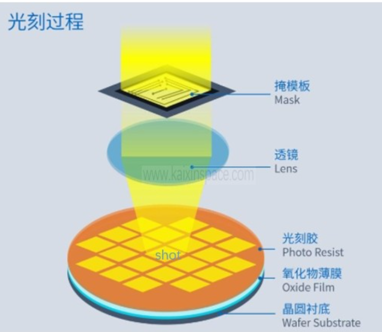
Mask fabrication plays a crucial role in tape-out. Through photolithography technology, the designed chip structure is accurately projected onto the surface of the silicon wafer. This process is akin to creating a precision mold, with subsequent manufacturing processes relying on it to ensure that each structure of the chip can be accurately formed. The precision of the mask directly affects the performance and quality of the chip, so high-precision equipment and processes must be used during fabrication.
Photolithography technology is the key means of transferring patterns layer by layer onto the silicon wafer. After mask fabrication, photolithography technology is used to give different regions of the silicon wafer different characteristics, thereby constructing the complex structures required for the chip. The photolithography process must be conducted in a highly clean environment, and the precision and stability of the equipment are critically important to ensure the accuracy of pattern transfer.
Etching follows the completion of photolithography. The main purpose of etching is to remove the parts of the silicon wafer that are not protected by photoresist during the photolithography process, precisely shaping the microstructures required for the chip. For example, to form structures such as the source and drain of a transistor, etching processes are needed to remove excess silicon material. The precision of the etching process greatly impacts chip performance; excessive etching may damage the originally designed circuit structure, while insufficient etching may fail to form ideal circuit components, so parameters such as etching depth and uniformity must be strictly controlled.
Thin film deposition is an indispensable step in the tape-out process. Through physical or chemical methods, a thin film is uniformly deposited on the surface of the silicon wafer. This thin film can alter the properties and characteristics of the silicon wafer, such as forming insulating layers or conductive layers, laying the foundation for the formation of subsequent components like transistors.
Ionic implantation technology is used to inject specific materials into the surface of the silicon wafer, altering its conductivity and forming key components such as transistors. The dosage and energy parameters of ionic implantation need to be precisely controlled to ensure that the performance of the components meets design requirements.
Metalization aims to cover the surface of the silicon wafer with metal, connecting various parts of the circuit to form complete electronic components. This process must ensure good contact between the metal and the silicon wafer, as well as the precision and reliability of metal wiring, to guarantee effective signal transmission within the chip.
Chemical mechanical polishing comes into play after metalization; the deposition of the metal layer may cause the surface of the silicon wafer to be uneven, affecting subsequent process steps and chip performance. The chemical mechanical polishing process flattens the surface of the silicon wafer through a combination of chemical etching and mechanical polishing, ensuring that the surface meets the flatness standards required for subsequent processes, paving the way for chip testing and packaging.
Testing and packaging are conducted after completing the above series of process steps. The chips undergo rigorous functional testing to verify whether they meet the initial design requirements. Only chips that pass testing will enter the packaging stage. The purpose of packaging is not only to protect the chips from external environmental influences, such as moisture and dust, but also to facilitate connections between the chips and other circuit boards, enabling them to function in various electronic devices.
5. Insights into the Economic Effects Behind Tape-Out
The fundamental reason for the high costs of tape-out lies in the small batch production model, where high mask and equipment costs need to be distributed across a limited number of chips.This results in high unit costs during the tape-out phase.However, once entering the mass production phase, the situation changes significantly.At this point, wafer costs become the primary source of costs, and as production scales up significantly, mask and equipment costs are distributed across a large number of products, leading to a substantial reduction in unit costs per chip.This clearly demonstrates the importance of economies of scale in controlling chip manufacturing costs.
However, the tape-out process is not always smooth; failures in tape-out can lead to severe economic consequences. If multiple consecutive tape-outs fail, a company may face significant financial losses due to massive investments, resulting in losses in manpower, resources, and funds, potentially leading to company bankruptcy.Therefore, tape-out represents both a test of technical strength and a severe economic challenge for chip manufacturing companies.
6. Innovative Paths to Reduce Tape-Out Costs
To effectively reduce tape-out costs, Multi-Project Wafer (MPW) technology has emerged. The core of MPW technology is to integrate multiple integrated circuit designs that use the same process onto the same wafer for tape-out.After manufacturing, each design can obtain dozens of chip samples, which is sufficient for experiments and testing during the prototype design phase.Through the MPW tape-out method, all participating projects only need to share costs based on chip area, and this cost is only 5% – 10% of the full mask tape-out cost.This technology has significantly reduced the cost risks in the product development process, providing an economical and efficient solution for small batch production, allowing many companies to attempt and validate chip development at a lower cost during the early stages.
In summary, tape-out, as a key step in the chip manufacturing process, has profound impacts on the cost, time, process, and economic effects, all of which significantly influence the development of the chip industry. A deep understanding of all aspects of tape-out is crucial for promoting advancements in chip technology and the healthy development of the industry.
We welcome everyone to engage in discussions, and I consistently share valuable insights on chip manufacturing daily. Your attention, likes, and views are my motivation to continue creating high-quality articles. Thank you!We welcome everyone to engage in discussions; long press the image to add WeChat and join the group, noting your name + company + position.
Exciting Knowledge Recap:
Overview of Silicon Nitride Films in Advanced Chip Processes
Detailed Explanation of Advanced Process SiCoNi Pre-Cleaning Technology
Comprehensive Analysis of Dummy Structures in Semiconductor Manufacturing: Types, Functions, and Application Scenarios
Clarifying Mainstream Strain Silicon Technology in One Go, Full of Insights
Why Gallium Nitride Can Rewrite the Charging Era: Insights into the Rise of Third-Generation Semiconductors from Charger Competition
Why is it Necessary to Deposit Ti and TiN Films Before Tungsten Deposition in Advanced Nano Contact Processes?
How to Choose Suitable Bandgap Materials in Chip Manufacturing
The Most Comprehensive Compilation of Common FAB Terminology, Extending Over Six Thousand Words
Essential Terms for Entering the Semiconductor Industry, Do You Know Them All?
Why High Doping Causes “Traffic Jams” in Semiconductors? – A Simple Explanation of Carrier Mobility Reduction
LVT, RVT, and HVT in Chips: How Threshold Voltage Shapes Chip Performance and Power Consumption?
What are N-Type and P-Type Wafers? A Comprehensive Explanation.
The Whole Internet is Searching! The Role of 12-Inch Wafer Notches Revealed + Knowledge Extension Insights