Intel: Microprocessor Chip
01
Intel 4004 Microprocessor
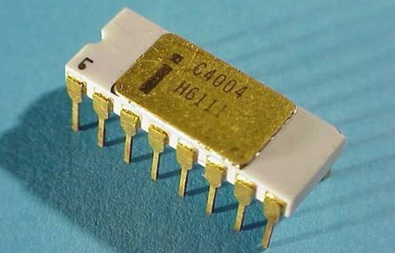
Release Date: November 15, 1971
Features: 10-micron process, 2250 transistors, speed 108KHz, size 3mm×4mm, 4-bit processor, 45 instructions, executes 50,000 instructions/second, priced at $200
The 4004 can read and execute instructions and exchange information with other computer components. It can perform 60,000 calculations per second, with a computing power 12 times that of ENIAC. The 4004 was the world’s first commercial processor, not the first microprocessor. The first microprocessor was developed by the U.S. military for the F-14 Tomcat fighter jet, consisting of six chips forming the Central Air Data Computer (CADC), although it was simpler than the 4004 and had a speed of only 9.15KHz. At that time, the Intel 4004 processor cost $200 each, laying the foundation for future system intelligence functions and personal computers.
Intel also developed the 4001 memory, 4002 read-only memory (ROM), and 4003 registers. Together with a keyboard and display, these could form a microcomputer system.
Moore considered the 4004 to be one of the most revolutionary products in human history. Before the 4004, the functions of chips were predefined. If one wanted to change the function, hardware had to be modified. Now, by changing the user instructions stored in the 4002, the 4004 could achieve different functions, leading to the birth of the independent software industry.
02
Intel 8008 Microprocessor
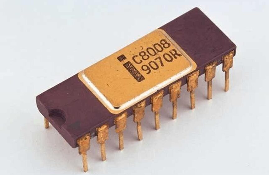
Release Date: April 1, 1972
Features: 10-micron process, 3500 transistors, 16KB memory, two speeds of 0.5MHz and 0.8MHz, size 3mm×4mm, 8-bit processor, 16-bit address bus, 16-bit data bus
Radio Electronics published an article in 1974 introducing a device using the 8008 called the Mark-8, recognized as the first home computer. Since the 8008 used a P-channel MOS microprocessor, it was still classified as a first-generation microprocessor. Intel began to have its own instruction technology during the 8008 processor era, marking another historical turning point.
The 8008 chip was originally designed for Datapoint in Texas, but the company did not have sufficient funds to pay for it. Thus, an agreement was reached whereby Intel retained all intellectual property rights to the chip and acquired the instruction set developed by Datapoint, which laid the foundation for today’s Intel x86 series microprocessor instruction set.
03
Intel 8080 Microprocessor
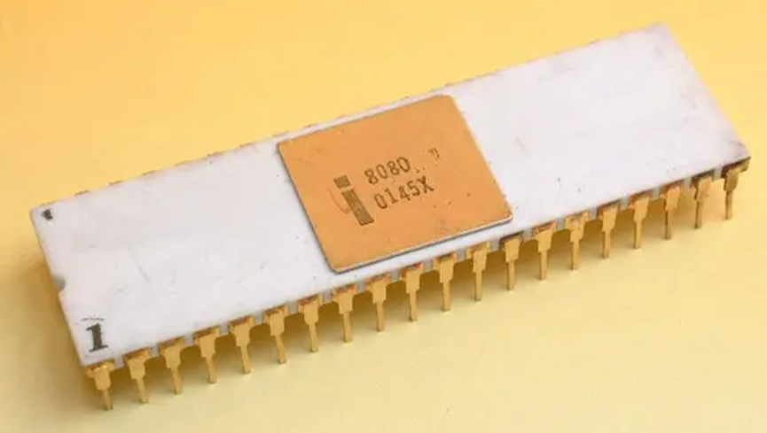
Release Date: April 1, 1972
Features: 6-micron process, 6000 transistors, 16-bit memory, 2MHz speed, 8-bit processor, 16-bit address bus, 8-bit data bus, 7 eight-bit registers
In 1974, the first commercial 8-bit single-chip microprocessor 8080 was designed by Faggin, truly pioneering the microprocessor market. The 8080 replaced P-channel with N-channel MOS circuits, marking the birth of the second-generation microprocessor.
Subsequently, a wave of computer enthusiasts began assembling computers at home in their garages, including Apple’s two founders, Stephen Wozniak and Steve Jobs. In 1976, the “Apple I” was born, the first pre-assembled home computer. The subsequent “Apple II,” equipped with a color display and external disk storage, became popular as a home computer for both office and gaming purposes.
In 1978, Apple II sold 20,000 units, and Apple quickly became a star company with annual sales exceeding $30 million. The rise of the home computer market attracted the attention of the Blue Giant, IBM. To rapidly develop a home computer that could gain market acceptance, IBM decided to implement an “open” policy, leveraging existing hardware and software from other companies. Due to its good relationships and better problem-solving solutions, Intel became IBM’s microprocessor supplier.
However, IBM also had a hand to play with Intel. To prevent Intel from monopolizing the market, IBM required Intel to license its CPU designs to others, leading Intel to license CPU technology to AMD. This provided a significant backdrop for AMD’s future development.
In 1981, IBM launched the IBM PC by mimicking the Apple II computer, forcefully entering the home computer market. From then on, the PC (personal computer) became synonymous with home computers. IBM’s orders caused Intel’s microprocessor sales to soar.
Faced with aggressive competition from Japanese chip companies, American chip companies were unable to cope. Even with the “U.S.-Japan Semiconductor Agreement” and the “Plaza Accord,” the U.S. ultimately failed to salvage its chip industry collapse. Under the Japanese’s aggressive strategy of “always pricing 10% lower,” Intel was unable to counterattack, and its memory market share plummeted, dropping to as low as 10%, with the latest 256K memory’s market share falling to just 1%.
The process of strategic turnaround was quite brutal: in 1986, Intel closed 7 out of 8 factories, laid off 7,200 employees, and incurred losses exceeding $170 million. This was also the only loss Intel experienced since going public.
As it exited the memory business, Intel invested $300 million in R&D to create the 80386 (abbreviated as 386) microprocessor. The 386 was Intel’s first 32-bit processor, three times faster than the 16-bit 286 processor, while being compatible with it, and it also had multitasking capabilities, meaning it could run multiple programs at the same time.
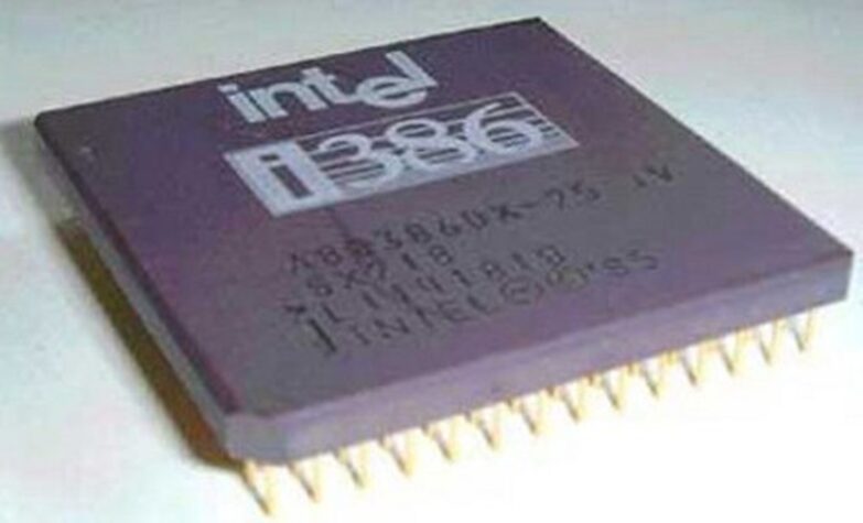
The 386 chip was a true milestone in computer technology; consumers began referring to their personal computers as “386,” as if this number were the brand of the computer. Meanwhile, Microsoft and other software developers began to favor this product.
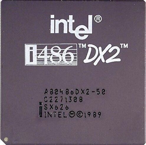
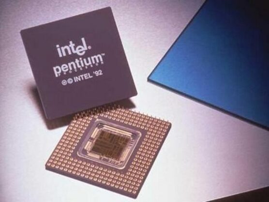
In 1989, Intel launched the 486 processor. In 1993, it introduced the groundbreaking Pentium processor. Since then, Intel’s microprocessors have continually doubled their performance every two years, leaving all competitors increasingly far behind.
In 1990, Microsoft’s Windows 3.0 operating system was designed to run on the 386 chip. From then on, Microsoft’s Windows operating system became increasingly powerful, with more and more code, and Intel had to continuously develop more powerful and faster microprocessors, or else the operation of the Windows operating system would slow down, with software in turn driving hardware advancements.
Thus, every time Microsoft released a new operating system, it brought a new round of business opportunities for hardware vendors such as microprocessors and memory. Microsoft and Intel thus formed a unique hardware-software alliance, dominating the personal computer era.
ARM: Mobile Processors
Computer programs ultimately need to be converted into a series of instructions to run on processors. Early processors, from IBM to Intel, aimed to implement as many instructions as possible during design. This approach has the advantage of being feature-rich and powerful, but the downside is design complexity, with each instruction taking different execution times, leading to unnecessary waits during processor operation and resulting in higher power consumption. This type of processor is categorized as “Complex Instruction Set Computer” (CISC).
In 1977, addressing the flaws of complex instruction sets, Professor David Patterson from the University of California, Berkeley, proposed the design philosophy of Reduced Instruction Set Computer (RISC), advocating for retaining only a few commonly used instructions while utilizing common instructions to combine more complex ones. This way, since the execution time of each instruction is the same, the processor’s operation becomes smoother, faster, and consumes less power. The reduced instruction set greatly simplified the design of computer processors, marking a revolution in the history of computer development.
To be cautious, Intel also attempted to launch the 80860 processor based on the reduced instruction set, but due to its incompatibility with the x86 architecture, it was not accepted by consumers, leading Intel to focus on developing complex instruction sets. Meanwhile, when Microsoft discovered that old rivals IBM and Apple were unexpectedly collaborating to develop a reduced instruction set operating system, it woke up and returned to the Wintel alliance.
Complex instruction sets also defeated reduced instruction sets in the workstation field. Continuous product iterations allowed Intel’s workstation processors to significantly outperform all processors in the reduced instruction set camp. Eventually, the six major workstation server manufacturers in the reduced instruction set camp, including IBM, Motorola, and HP, were completely defeated, and even Professor David Patterson had to add content about complex instruction sets in his textbooks.
Despite not prevailing in the personal computer era against the solid Wintel alliance and exiting the personal computer and workstation fields, the reduced instruction set made a comeback in the mobile era, firmly establishing its dominance. The fundamental reason is that complex instruction sets have a fatal flaw: they consume too much power.
In the personal computer era, consumers did not feel much about power consumption. Taking Intel’s Core processor as an example, if used continuously day and night, its annual power consumption is equivalent to its price. This level of power consumption is unbearable for smartphones and tablets in the mobile era, highlighting the advantages of the reduced instruction set’s low power consumption.
In 1978, the second year after the reduced instruction set was born, a company called Acorn Computers was founded in Cambridge, UK. Acorn developed a 32-bit, 6MHz processor using its own instruction set based on the reduced instruction set and named it ARM (Acorn RISC Machine).
In the 1980s, Acorn collaborated with Apple to develop a new version of the ARM microprocessor core, as Apple wanted to use ARM to develop chips for the Newton handheld computer. In 1990, after obtaining investments from Apple and VLSI Technology, Acorn established a subsidiary called ARM, dedicated to developing low-cost, low-power, high-performance chips.
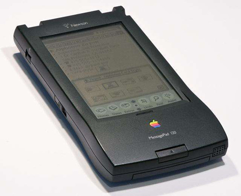
Due to the failure of the Newton handheld computer (a product launched by Apple when Jobs left) and its own limited strength, ARM could not sell chips directly and was forced to take a new path: it does not produce chips, nor does it design chips, but licenses the chip architecture’s intellectual property (IP) cores to other companies.
In the intellectual property licensing model, one-time technology licensing fees (usually in the millions of dollars) and royalty commissions (usually 1%–2%) are the main sources of ARM’s revenue.
Major chip design companies purchase ARM microprocessor cores from ARM and add appropriate peripheral circuits as they develop towards niche markets, building microprocessor chips that meet market needs. Through this cooperative ecosystem, ARM quickly dominated the global architecture of reduced instruction set microprocessors, allowing its clients to save resources in designing microprocessor cores and relatively quickly enter the chip design market.
ARM, similar to TSMC, which was established three years earlier, is a product of specialized division of labor in the semiconductor industry chain. Together, they form the “IP licensing + Fabless + Foundry” model for mobile smart products, benefitting almost all smartphone brands in the market today, from Apple and Huawei to Xiaomi. Based on the integration advantages of mobile system chips, the number of companies collaborating under ARM architecture licensing has reached thousands. As of 2020, ARM partners have shipped over 160 billion ARM architecture-based chips.
Moreover, the ARM architecture, which has already established an absolute advantage in the mobile field, has begun to invade the desktop and laptop markets, with more and more computers adopting CPUs based on the ARM architecture. In June 2020, Apple announced that its computers would switch to self-developed chips based on the ARM architecture, abandoning the x86 architecture it had used for fifteen years. Qualcomm is also collaborating with HP, Lenovo, and Asus to launch computers using ARM architecture Snapdragon chips.
The software ecosystem that x86 relies on for survival is not a problem in ARM’s eyes. The mobile applications built on the ARM architecture have reached millions, rivaling the applications available on computers. Even Microsoft has declared it will support ARM architecture starting with Windows 8.
ARM architecture has even penetrated the server processor market, gradually shifting its development focus to data centers, smart cars, and the Internet of Things. Compared to the x86 architecture, the ARM architecture has the advantage of openness, allowing it to license intellectual property cores to clients and develop diversified chip products, making it more suitable for complex application scenarios like the Internet of Things.
In January 2019, Haisi released its first server chip based on the ARM architecture—the Kunpeng 920, which will partially replace Intel’s server chips, significantly reducing Huawei’s data center operating costs. By the end of the year, Amazon announced that its own servers would use the ARM-based next-generation architecture NEOVERSE N1 processor chip GRAVON2, which could save customers up to 40% in costs. Major server companies like Google and Alibaba Cloud are also collaborating with chip design firms like Qualcomm and AMD to promote ARM architecture as an “Intel alternative.”
ARM inadvertently, along with TSMC, completed a revolution in the chip industry: they each reshaped the architecture design at the top and chip manufacturing at the bottom. Today, ARM occupies 95% of the architecture design for smartphones and tablets, while TSMC holds half of the global wafer foundry market, forming a monopoly pattern that is distinctly different from the Wintel alliance.
Both ARM and TSMC were born on small islands, which does not seem coincidental. It is precisely because they lack broad market support that these two companies were forced to pursue specialized division of labor, seeking orders globally and growing from small companies into international giants.
NVIDIA: Parallel Processors
In 1993, 30-year-old Jensen Huang and two engineers saw the potential in the video game computing market and founded NVIDIA with $40,000 in startup capital.
In the following four years, NVIDIA launched two chips. Due to misjudging the technological direction, both products failed, and the company was on the brink of collapse. Jensen decided to shift the company’s focus from game consoles to the emerging personal computer market and recruited Dr. David Kirk from the game design company 3Dfx to serve as chief scientist, organizing a large R&D team. NVIDIA’s third chip adopted Microsoft’s graphics card standard, gaining Microsoft’s favor and achieving great success.
Early graphics cards only contained simple memory and frame buffers, serving primarily to store and transmit graphics, with all operations controlled by the CPU. In the 1990s, some engineers realized that rendering images on the screen was essentially a task that could be parallel processed—each pixel’s color could be calculated independently without considering other pixels. This led to the birth of the GPU, which became a more efficient graphics processing tool than the CPU.
In 2000, when launching the second generation of GPUs, Jensen boldly proposed his “Huang’s Law”: graphics card chips double their performance every six months. Thus, NVIDIA upgraded its products every six months according to this strategy, surpassing many competitors and ultimately becoming the leader in graphical computing.
CPUs are suitable for multi-functional task processing, capable of performing sequential calculations step by step, currently achieving dozens of cores with existing technology. In contrast, GPUs are designed for large computations, operating in a highly parallel manner, achieving thousands of cores. CPUs are general-purpose and adaptable to all scenarios, while GPUs possess extremely powerful performance in certain areas of large computations, outperforming CPUs by dozens or even hundreds of times.
Today, graphics cards generally use GPUs as the main processing unit, significantly reducing the burden on CPUs and enhancing the display capabilities and speeds of computers. Some professional graphics cards have more transistors than contemporary CPUs. GPUs have redefined modern computer graphics technology, greatly promoting the development of the personal computer gaming market.
The computational power of GPUs is so strong that they can be utilized for more than just graphics processing; for example, quantitative traders on Wall Street use NVIDIA’s GPUs for trading. These individuals often face the complexities of GPU programming. In 2003, Kirk persuaded Huang to vigorously develop the Compute Unified Device Architecture (CUDA) technology. CUDA supports parallel computing in a C language environment, meaning engineers can easily write programs based on the CUDA architecture and effortlessly use GPUs for parallel computations.
GPUs have transformed into General-Purpose Graphics Processing Units (GPGPU), capable of handling non-graphical general computing tasks. GPGPUs possess powerful parallel processing capabilities, allowing them to significantly exceed traditional CPUs when the computational workload far exceeds the needs for data scheduling and transmission. Once CUDA technology matured, Kirk again persuaded Huang to ensure that all of NVIDIA’s future GPUs must support CUDA.
In 2007, NVIDIA officially launched the CUDA architecture Tesla GPU, and almost overnight, supercomputers around the world adopted Tesla GPUs for computation.
In 2012, the rise of deep learning brought new breakthroughs in artificial intelligence. Deep learning computations based on massive data require cloud-based completion and then intelligent inference on new input data through algorithms at the terminal. AI chips are divided into two main categories: cloud training chips and terminal inference chips, with GPUs being the most commonly used cloud training chips. For the same computational workload, GPUs have significant advantages in both price and power consumption compared to traditional CPUs.
Currently, there are about 3,000 AI startups worldwide, most of which use NVIDIA’s hardware open platform. This is akin to how people in the 1990s started businesses based on Windows or how people in the early 21st century started businesses on Android and iOS.
Jensen Huang confidently claims that NVIDIA is not only riding the wave of artificial intelligence but is also a crucial reason for the formation and advancement of this wave. NVIDIA holds 80% of the market share for cloud training chips.
Benefiting from the strong demand for processing power in data center processors due to AI applications, NVIDIA’s data center business began explosive growth starting in 2016, with growth rates exceeding 100% for seven consecutive quarters.
The global data volume is growing at an annual rate of about 40% and continues to rise. However, the performance improvement of CPUs has slowed down and can no longer keep pace with the growth of data. In contrast, the number of transistors in GPUs is still increasing exponentially, allowing GPU performance to improve at a rate of about 40%, keeping up with the data explosion pace.
In addition to occupying a significant share of the cloud training chip market, NVIDIA is also making moves in the terminal inference chip market. The largest market for terminal inference chips is automotive chips, and NVIDIA has launched autonomous driving solutions, selling a large number of hardware to automakers such as Tesla, Audi, and Volvo, as well as automotive technology suppliers like Google and Bosch. Besides first-tier automakers, NVIDIA also supplies autonomous driving kits to over 100 startups.
On July 8, 2020, a watershed historical event occurred: NVIDIA’s market value approached $250 billion, surpassing Intel for the first time, becoming the largest semiconductor company in the U.S. Multiple media outlets eagerly announced: one era ended, and another began. As of now, NVIDIA’s market value is approximately $647 billion, nearly five times that of Intel.
Source: Toutiao, Freedom Comes From
Images from publicly available online data searches