 New Opportunities in the Semiconductor IndustryMaterial Innovation as the Key to Breakthroughs
The global semiconductor industry is entering a dual transformation period characterized by technological breakthroughs and ecological restructuring. The demand for AI computing power is surging, and localization alternatives are entering deep waters, significantly increasing the strategic value of equipment and materials. On September 4, the 2025 Semiconductor Manufacturing and Materials Chairman Forum was held in Wuxi, where leading entrepreneurs gathered to explore paths for industry breakthroughs.
01
Industry Collaboration Welcomes Transformation
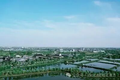
Gu Guodong, Deputy Secretary of the Party Working Committee of Wuxi High-tech Zone, emphasized in his speech that Wuxi High-tech Zone, as an important carrier of the integrated circuit industry, bears the mission entrusted by the state. From the “908 Project” to the national microelectronics base, Wuxi has always been at the forefront of the industry, implementing special policies to support enterprise recruitment, R&D investment, and talent subsidies, striving to create fertile ground for innovation and entrepreneurship in the integrated circuit industry. Gu stated that addressing the pain points and difficulties of the industry is a top priority for the government, and Wuxi will continue to provide comprehensive support for enterprises.
Lin Jian, Secretary-General of the Semiconductor Materials Branch of the China Electronic Materials Industry Association, proposed that the focus should be on third-generation and wide-bandgap semiconductor materials to accelerate the process of self-control. He called for the establishment of an integrated research system encompassing “materials—equipment—processes—software,” improving talent training mechanisms, strengthening industry chain collaboration, promoting standardization and internationalization, and building a multi-source supply chain. These five paths will inject strong momentum into the high-quality development of China’s semiconductor industry, helping enterprises gain an advantage in global competition.
02
Technological Breakthroughs Drive Growth
Han Jianglong, Chairman of Jiangsu Huahai Chengke, pointed out that epoxy molding compounds (EMC), as the core material for integrated circuit packaging, are entering a new growth cycle driven by localization alternatives, automotive electronics, and advanced packaging technology upgrades. Different packaging technologies impose differentiated requirements on material performance, and technological iterations not only expand market size but also drive the demand for high-end products, providing broad opportunities for enterprises with R&D capabilities. Huahai Chengke has achieved a breakthrough in global shipments, ranking second.

Qi Hongji, Chairman of Hangzhou Fujia Gallium Industry, shared the industrialization progress of gallium oxide materials. Gallium oxide, with its wide bandgap and high breakdown field strength, holds significant strategic importance in fields such as energy and national defense. He emphasized that AI-assisted intelligent equipment is key to the large-scale application of gallium oxide, and Fujia Gallium has broken through the 6-inch guided mold growth technology, achieving “one-click crystal growth” through “AI + crystal equipment.” This innovation marks a significant breakthrough for China in the field of wide-bandgap semiconductor materials.
03
Exploration of Self-Control in the Industry Chain
During a roundtable discussion, Bao Wenzhong, Chairman of Yuanjiwei, stated that the industrialization of two-dimensional semiconductor materials has reached the “final step” stage. As the performance improvement of silicon-based processes slows down, major companies like Samsung and TSMC are laying out two-dimensional materials, while domestic enterprises are accelerating the industrial transformation of university research results. Yu Zhenrui, President of Jidian Energy, believes that perovskite new materials will reshape the photovoltaic industry chain, as their solution-based processing significantly reduces costs and shows potential in diverse scenarios. These technological breakthroughs provide new paths for self-control in the industry chain.
Chen Xin, VP of Zhaosheng Micro, emphasized that enterprises need to continuously invest resources and build a stable ecosystem with suppliers to address common issues such as efficiency and cost. Chen Jinlong, VP of Yake Technology, shared experiences of achieving technology digestion through mergers and local factory establishment, with the company completing three mergers to form a core product line. Xu Wei, VP of Changjing Technology, pointed out that delivering quality products and accurately meeting customer needs is key, and a localized business cooperation system must be established to participate in international competition. These practices provide valuable experiences for collaborative innovation in the industry chain.
04
Accelerating Innovation in Materials and Equipment
Zheng Xiaobin, Chairman of Tiantong Holdings, introduced the application potential of sapphire wafers in advanced packaging and power semiconductor fields. Sapphire plays an important role in the rise of third-generation semiconductors due to its high hardness and thermal stability. Guo Jianyue, former General Manager of Hangzhou Zhongxin Wafer, predicted that 12-inch large silicon wafers will experience rapid growth due to AI demand, and the localization rate in China will continue to rise. By 2026, the global market may shift to a state of supply shortage, bringing development opportunities for domestic enterprises.
Zhang Lijuan, Chairman of Shanghai Xinqian, stated that the company’s CMP polishing pads have overcome the challenges of the 7-nanometer process, marking a transition for the domestic new materials industry from “meeting basic needs” to “high-quality development.” Xu Yanqing, General Manager of Honeywell China, emphasized that enterprises need to seize the opportunity of rising equipment investment in China and become industry enablers. These innovative achievements demonstrate China’s rapid progress in semiconductor materials and equipment, laying a solid foundation for self-control in the industry chain.
05
Global Layout and Future Outlook
Xu Jie, Editor of Caixin, pointed out in his speech that the global semiconductor industry is entering a dual transformation period, with the strategic value of equipment and materials significantly increasing. The escalation of U.S. export controls against China is forcing China to accelerate the construction of a self-sufficient industry chain, making technological breakthroughs a national security issue. He emphasized that enterprises need to grasp the two major trends of accelerated technological iteration and deepened supply chain restructuring, seeking new opportunities in global layouts. This judgment points the way for industry development.
Forum guests generally believe that the future semiconductor industry will exhibit a parallel trend of “technological breakthroughs” and “ecological restructuring.” On one hand, new technologies such as AI and 5G will drive continuous innovation in equipment and materials; on the other hand, industry chain collaboration and multi-source supply chain construction will become core competitiveness for enterprises. Industrial clusters like Wuxi High-tech Zone will support enterprises in making the leap from technological breakthroughs to commercialization through policy support and ecological construction. The Chinese semiconductor industry is at a critical turning point from following to catching up.
Source: Caixin, Dongfang Caifu, etc.
END

Hosts: Hangban, Danyang, Lin Shuo, Lu Yi
Organizer: Zhang Yumei Reviewed by: Ruo Wen
Final Review: Lai Ting