
Click
Attention
References
Document Title:Calibration Testing Method for Multi-Degree-of-Freedom Capacitive Sensors Based on Inertial Sensors
Authors:Li Dongxu, Wang Shaoxin, Qi Keqi, et al.
Source:Chinese Science: Physics, Mechanics, Astronomy, 2024, 54: 270407
DOI:10.1360/SSPMA-2024-0090
01
Abstract
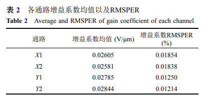
The capacitive sensor is a key component for achieving high-precision displacement detection in space missions. Influenced by the processing errors of the sensitive structure and the accuracy of electronic devices, this paper analyzes the theoretical model of the capacitive sensing circuit with a differential amplifier circuit as the core, and constructs its gain and zero-offset models based on this analysis. Calibration experiments were conducted in conjunction with a prototype of the sensitive structure, achieving precise and efficient calibration of displacement to voltage in multiple degrees of freedom. The results show that, without temperature control adjustments, the calibration gain coefficients obtained from multiple tests across all channels have a Root Mean Square Percentage Error (RMSPER) value of less than 0.2‰.
02
Introduction
Inertial sensors are one of the important payloads for precise detection tasks in space, primarily applied in global gravity field measurement, verification of the equivalence principle, and detection of gravitational waves in space. The main role of capacitive sensing is to detect the relative position relationship between the test masses (TM) and the electrode holder (EH), providing input for subsequent precise control of the system. In practical applications, we find that due to the accuracy of electronic devices and processing errors of the sensitive structure, there is often a discrepancy between the theoretical gain and the actual gain of the capacitive sensing circuit (hereinafter referred to as “the circuit”). Additionally, due to the uniqueness of space missions, a ground calibration system needs to be established before orbital operations to calibrate the actual gain of the circuit. This paper proposes a new calibration method based on this foundation, connecting the circuit to the sensitive structure prototype, utilizing the continuous adjustment capability of the PI multi-degree-of-freedom drive controller to control the electrode holder to perform sinusoidal motion along a single-axis direction, and calibrating by detecting the sensing voltage at the same frequency as the sinusoidal motion, achieving high-precision conversion from displacement to voltage while reducing 1/f noise interference. Meanwhile, this paper also proposes a theoretical model for the zero-offset of the circuit and experimentally verifies the correctness of the model.
03
Working Principle and Model Construction
The precise measurement process of the capacitive sensor involves the conversion from displacement signal to capacitance signal, and then to voltage signal. The main working principle is: the relative displacement between the sensitive structure’s TM and EH is converted into a differential capacitance signal; the differential capacitance signal is connected to the circuit, an excitation is applied, and a response voltage signal is obtained. The structure of the circuit is shown in Figure 1, where the electrodes (Electrode cage, ET) attached to TM and EH form the differential capacitance, achieving the conversion from displacement signal to differential capacitance signal; the differential amplifier circuit (Differential amplifier, DAC) is used to sense and amplify the differential capacitance signal, generating a voltage signal; the frequency selective amplifier (Frequency selective amplifier, FSA) primarily amplifies the signal at the excitation frequency while suppressing high and low-frequency noise; the demodulation circuit (Demodulation circuit, DMC) consists of a multiplier and a low pass filter (Low Pass Filter, LPF), mainly used to demodulate the signal at the excitation frequency to obtain the amplitude of the sensing voltage. The high-frequency excitation signal (AC) serves two main purposes: on one hand, it provides high-frequency excitation to the circuit, achieving frequency division multiplexing of the detection and control circuits; on the other hand, it modulates and demodulates the signal to avoid the influence of 1/f noise. The analog-to-digital converter (Analog-to-digital converter, ADC) primarily collects data for subsequent digital control.
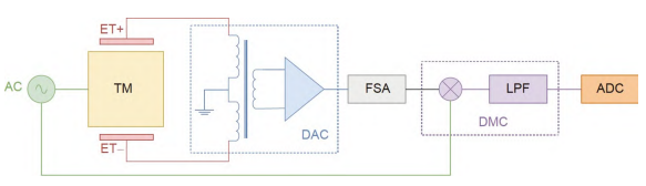
Figure 1Sensor Circuit Structure Diagram
1. Displacement Detection Principle
The sensitive structure mainly consists of EH and TM, with ET attached to the inner side of EH, where the distribution of the test mass and electrodes is shown in Figure 2. The TM is located at the center of EH, designed as a cubic structure. Each plane of EH has two sensing electrodes, forming six pairs of differential sensing paths to achieve real-time sensing of the relative position relationship between TM and EH in six degrees of freedom. The positive direction of each coordinate axis is defined as the positive electrode of each pair, and vice versa for the negative electrode. The sensitive structure detects the relative displacement between ET and TM by the influence on the differential capacitance value caused by their relative position change, as illustrated in Figure 3.
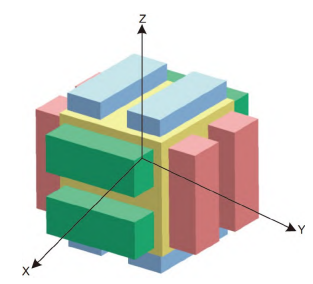
Figure 2Distribution of TM and ET in the Sensitive Structure
TM is located at the center, ET is attached to the outside
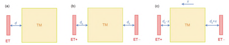
Figure 3Displacement Detection Principle Diagram
2. DAC Model
In the circuit principle diagram of capacitive detection shown in Figure 1, the most critical part is the DAC, which is the core of detecting differential capacitance. This paper references the integrated circuit design from the literature, considering only the influence of the excitation signal. The designed DAC structure is shown in Figure 4, which mainly consists of a sensing bridge and a charge amplifier. Here, Ui is the amplitude of the excitation signal, Cm is the nominal capacitance, ΔC is the change in one-sided capacitance caused by the displacement of the test mass, Cs is the stray capacitance to ground of the coaxial cable, Rb is the feedback resistance for controlling voltage, Cp is the isolation capacitor that prevents the control voltage from coupling into the sensing path, L is the inductance of the coil, and Cg is the isolation capacitor to prevent saturation of the charge amplifier. The feedback path of the charge amplifier is formed by Cf and Rf. In this model, the internal resistance of the transformer coil and the distributed capacitance of the coil are ignored. To facilitate modeling analysis, the circuit is simplified by treating the left side port of the differential transformer secondary as a Thevenin equivalent circuit.
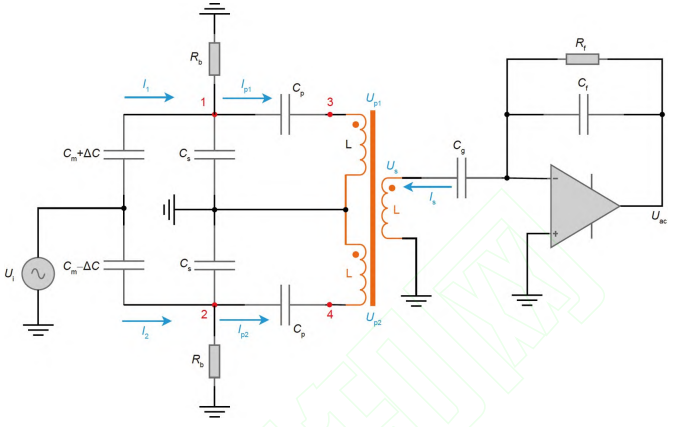
Figure 4 DAC Principle Diagram
04
01
Circuit Calibration
This paper developed a corresponding electronic system based on the above principles and conducted research on its gain coefficient calibration and the verification of the proposed zero-offset model. For the former, a modulation calibration scheme is proposed, which theoretically can greatly reduce the interference of low-frequency noise on the calibration results, improving the stability of the calibration results; for the latter, a zero-offset voltage testing method using positive and negative wiring is proposed to verify the zero-offset model.
Gain Coefficient Calibration:
1. Calibration System
For the calibration of the gain coefficient, a six-degree-of-freedom calibration system is designed, with its hardware structure shown in Figure 5, mainly consisting of an alignment adjustment mechanism, a six-degree-of-freedom piezoelectric platform, a sensitive structure, a circuit box, a DC power supply, and a PI controller. The alignment adjustment mechanism includes three parts: an inclination adjustment mechanism, a translational adjustment mechanism, and a rotational adjustment mechanism. The inclination adjustment mechanism is fixed to the base of the calibration platform, while the rotational and translational adjustment mechanisms are connected to the base via connecting arms. The alignment adjustment mechanism can achieve preliminary alignment of the relative position between TM and EH in six degrees of freedom, controlling TM to be as close to the center of EH as possible. The six-degree-of-freedom piezoelectric platform uses a piezoelectric ceramic displacement platform from PI, fixed to the inclination adjustment mechanism by screws. The PI controller can control the piezoelectric platform to achieve quantitative precise motion in six degrees of freedom, adjusting the relative position between TM and EH quantitatively in six degrees of freedom, while the piezoelectric platform can generate motion trajectories as needed, which is the basis of the research method described in this paper. The sensitive structure consists of EH and TM, where EH is fixed to the piezoelectric platform, and TM is connected to the rotational adjustment mechanism via a rigid column. The electrode holder (ET) is installed inside the electrode cage to sense the relative position relationship between EH and TM. The excitation voltage required for sensing is applied through a coaxial cable at the connection point between the rigid column and the rotational adjustment mechanism, and is applied to TM through the column. Each ET is connected to the sensing circuit inside the circuit box via coaxial cables, enabling real-time sensing of six channels.
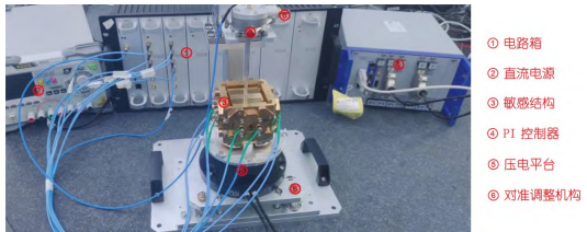
Figure 5 Six-Degree-of-Freedom Calibration System
05
Comprehensive Calibration Experiments
1. Gain Coefficient Calibration
In this paper, calibration experiments were conducted for four channels along the X and Y axes. Before the experiments, the alignment and fine-tuning control described in section 3.1 were used to position TM at the center of EH. Utilizing the continuous adjustment capability of the PI controller, the electrode holder was controlled to perform sinusoidal motion along the X and Y axes with a frequency of 1 Hz and an amplitude of 30 μm. The output voltage values were collected by the upper computer, with a sampling frequency of 50 Hz and a sampling time of 5 minutes. To verify the stability of the calibration scheme, five consecutive tests were conducted. According to the scheme designed in section 3.2, the carrier frequency range was selected as [0.99985, 0.9999] Hz, with a frequency step of 10−7 Hz and an initial phase step of 0.005. The mean peak voltage response curves of each channel under five sets of tests were plotted against the carrier frequency, as shown in Figure 6. It can be seen that, influenced by environmental fluctuations, circuit noise, and frequency errors of the piezoelectric platform, the frequencies at which the maximum sensing voltage was obtained showed slight differences across the test groups, but all remained within the selected range. During the tests, Ui was optimized to 5 V, and the gain coefficient test values for each channel were determined as shown in Figure 7 based on equation (32).
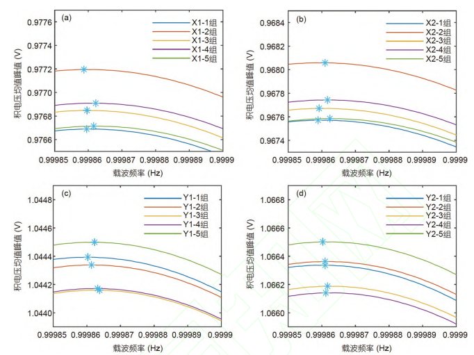
Figure 6 Mean Peak Voltage Response Curves of Each Channel
(a) X1 channel; (b) X2 channel; (c) Y1 channel; (d) Y2 channel
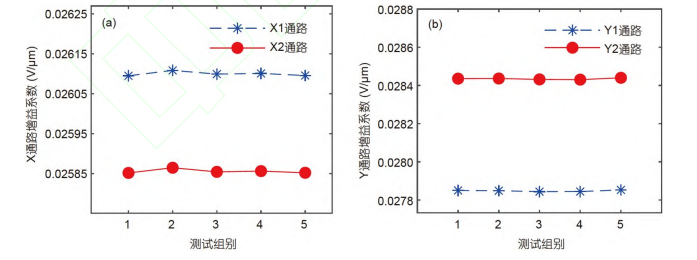
Figure 7 Gain Coefficients of Each Channel Under Five Tests
(a) X channel; (b) Y channel
2. Zero-Offset Model Verification
For the first characteristic, the PI controller was used to control the electrode holder to move along the X-axis by 0, ±5, ±10 μm, measuring the zero-offset voltage at different x positions. To ensure generality, tests were conducted at excitation voltage amplitudes of 2.5, 3, and 3.5 V, with a data sampling time of 5 minutes and a sampling frequency set to 100 Hz. The sampled data was averaged, and the zero-offset voltage values under various conditions are shown in Figure 8. It can be observed that when the piezoelectric platform generates different displacements along the X-axis, the measured zero-offset voltage values remain stable, thus verifying the characteristic that zero-offset voltage is independent of displacement x. For the second characteristic, by providing different excitation voltage amplitudes, the zero-offset voltage values of the sensing circuit were measured under different excitation voltage amplitudes using the same method, resulting in the curve shown in Figure 9. It can be seen that the experimental fitting curve of excitation voltage amplitude versus zero-offset voltage closely matches a quadratic function curve, fully verifying the circuit characteristic that zero-offset voltage is proportional to the square of the excitation voltage.
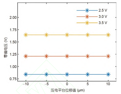
Figure 8 Zero-Offset Voltage Obtained at Different Displacements of the Piezoelectric Platform Under 2.5, 3, and 3.5 V Excitation Voltage
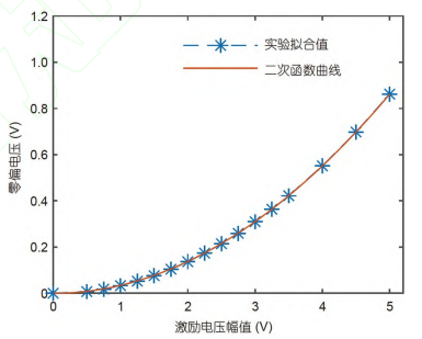
Figure 9 Zero-Offset Voltage vs. Excitation Voltage Amplitude Response Curve
06
Conclusion
This paper effectively calibrated the gain coefficients of the capacitive sensing circuit of the inertial sensor along four channels in two axes based on the sinusoidal motion output capability of the six-degree-of-freedom piezoelectric platform. The RMSPER values of the continuous five calibration values obtained for each channel were all less than 0.2‰. Additionally, a theoretical model for the zero-offset coefficient of the circuit was proposed and experimentally verified. Due to insufficient consideration of the motion stability of the piezoelectric platform during sinusoidal motion, future research can introduce a higher precision measurement system to monitor the output displacement of the piezoelectric platform in real-time, which is expected to further improve the calibration accuracy. The calibration results indicate that the gain coefficients obtained from actual tests show slight differences from theoretical values, primarily caused by parameter differences in circuit components and processing errors in the sensitive structure. The weight of these two factors in the differences in gain coefficient calibration still requires further research.
BME
Previous Reviews
Previous Recommendations
● Sensors for Motion and Posture Change Recognition
● WNTA5 Mediated miR-374a-5p Regulates Vascular Smooth Muscle Cell Phenotype Transition and M1 Macrophage Polarization Affecting Intracranial Aneurysm Progression
● The Role and Mechanism of miRNAs in Abdominal Aortic Aneurysms: Signaling Pathways and Clinical Insights
Technical Services


——END——
This article is an original content of the 【BME Doraemon Science and Technology Innovation Park】 public account
Please indicate the source from 【BME Doraemon Science and Technology Innovation Park】 when reprinting
and add the original link at the end of the article
BME
Join the Original Article Exchange Group

This group aims to build a platform for cooperation and communication for students interested in the original article content of this public account or other public accounts, providing assistance for everyone’s research journey, helping every hardworking Nobita!
Friendly Reminder:To join the group, please note (format like School + Major + Name or XX Public Account + Name, thank you) You can first add the editor’s WeChat ID (zyzc12345678) or long press the QR code below, and in the application messagenote “Mali Zhiliang”, add the editor, and then enter the relevant group.

For submissions, collaborations, reprint authorizations, and other related matters
Please contact WeChat ID: zyzc12345678
or join the original article exchange group