 Literature from IMEC, published in 2022, focuses on the impact of BSPDN on PPAT.The front end (FEOL) is an active driver of chip power/performance/area (PPA). As scaling approaches the physical limits of semiconductor devices, the back end (BEOL)/middle end (MEOL)/packaging becomes increasingly important for PPA improvements in chips/systems. At 2nm and below, BSPDN back interconnects (beneath the chip/backside) have also been proposed to complement traditional back-end processes (BEOL).Two connection processes of nTSV-BPR after silicon thinning in BSPDN:
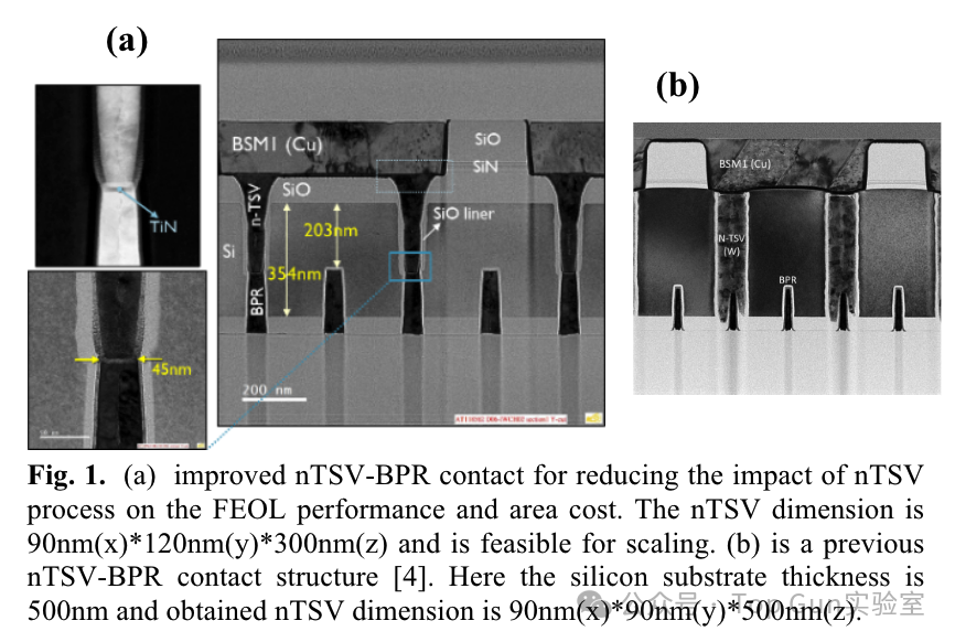 Schematic diagrams of FSPDN and BSPDN:
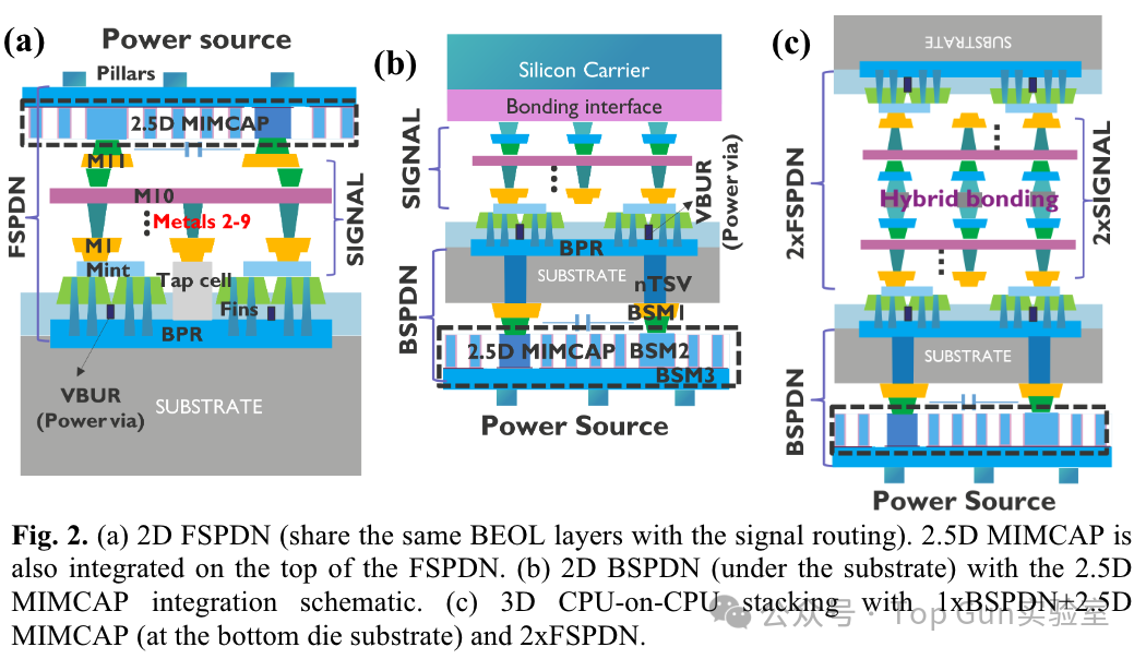 Design rules for FSPDN at the A14 node. FSPDN may lead to significant IR drop compared to BSPDN.
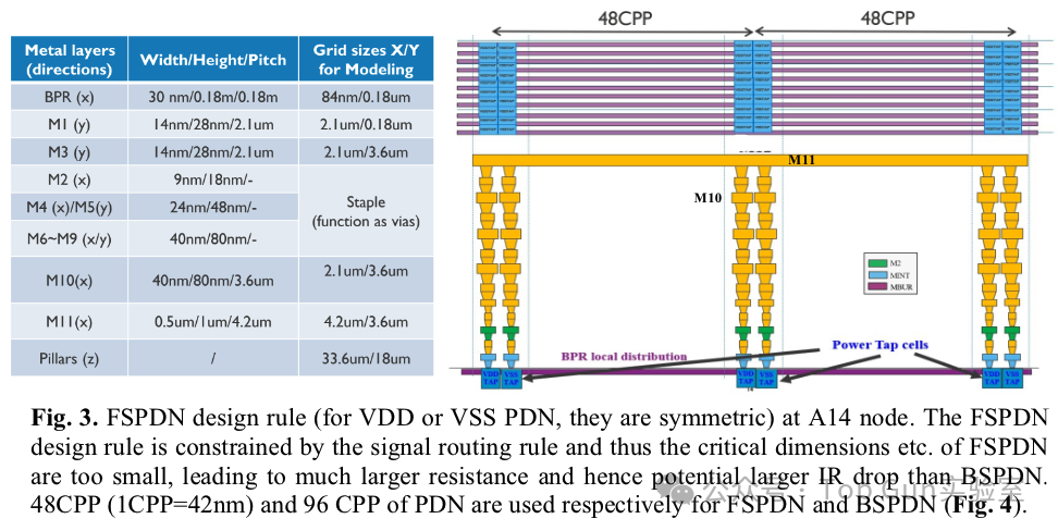 Design rules for BSPDN:
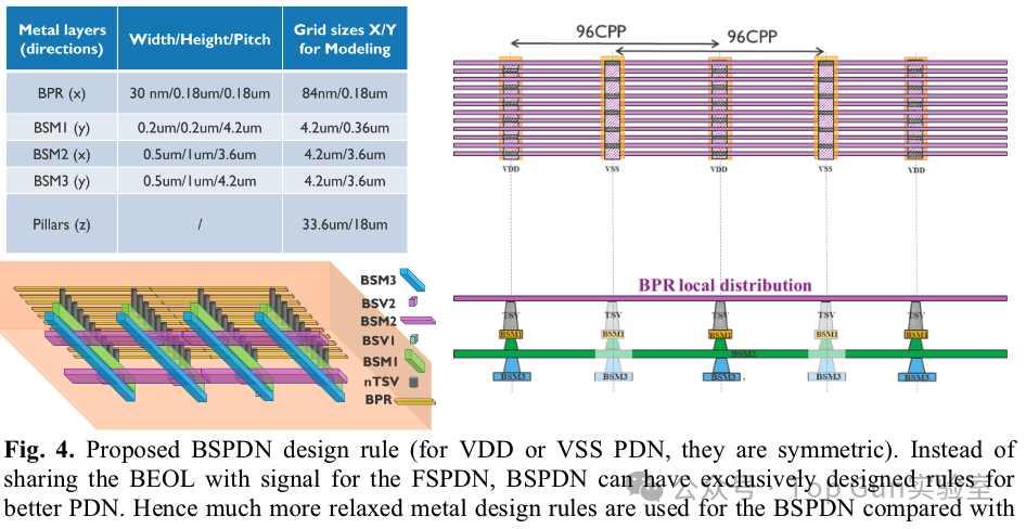 The author uses RO simulation to model the IR drop of the CPU.Voltage transient performance of BSPDN and FSPDN and the impact of 2.5D MIMCAP:
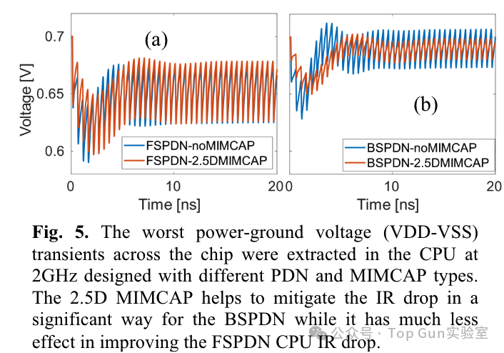 IR drop cloud map of FSPDN:
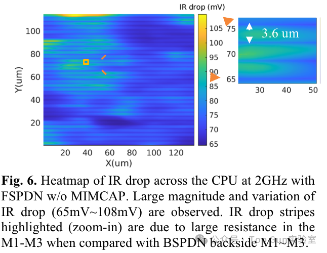 IR drop cloud map of BSPDN:
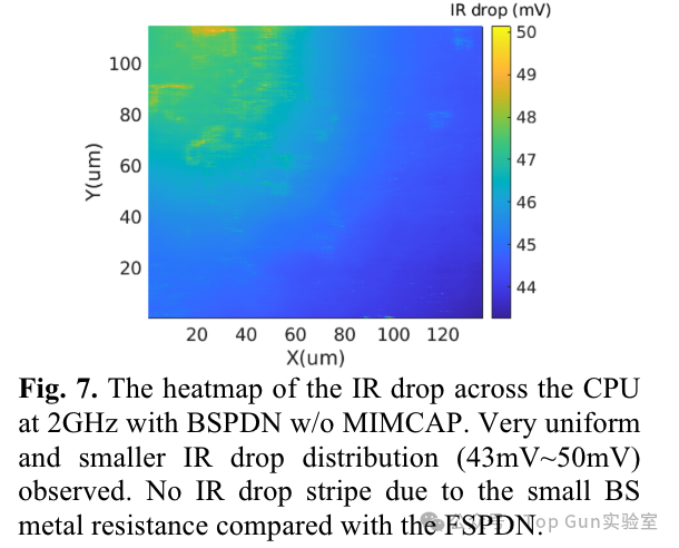 Summary of IR drop under different designs: (The IR drop of the 3D Die in the figure seems inconsistent with the description in the text)
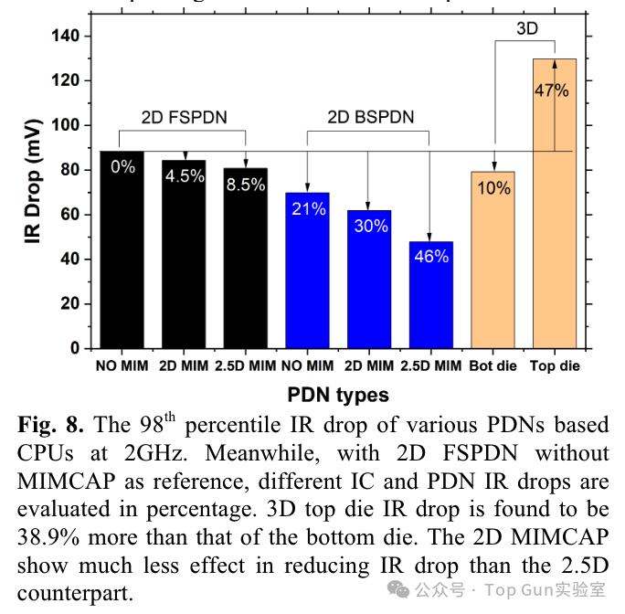 Analysis of the impact of IR drop on CPU timing based on RO simulation:
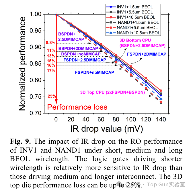 Power consumption of PDN under different designs:
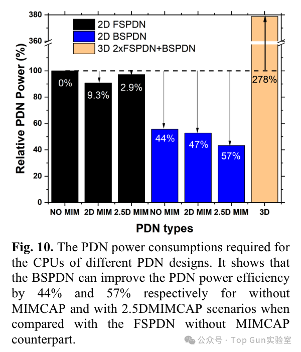 Physical design results under different PDN designs: BSPDN can save 8% area.
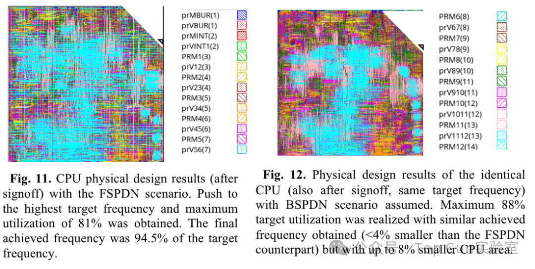
 The author conducts thermal simulation evaluation based on the FEM method.Thermal simulation model of BSPDN:
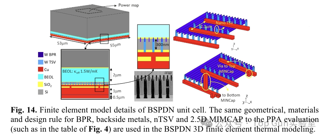 Package-level thermal model/boundary conditions/power map:
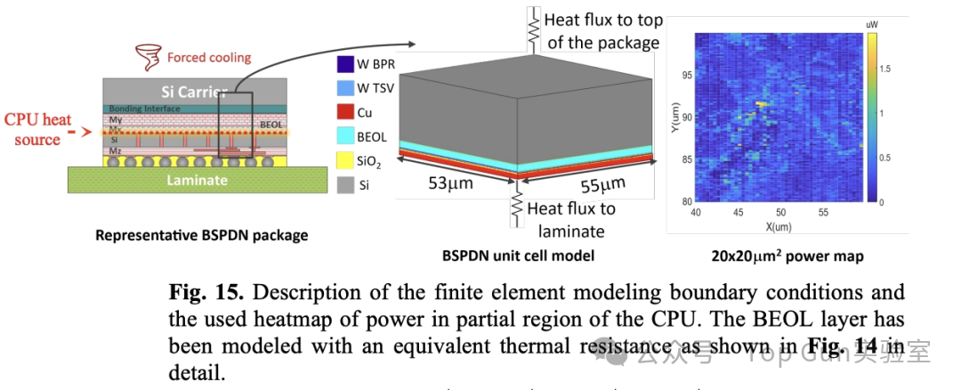 Due to the increase in vertical thermal resistance caused by BSPDN BEOL/Bonding, and the increase in diffusion thermal resistance due to silicon thinning, thermal performance is worse than FSPDN.
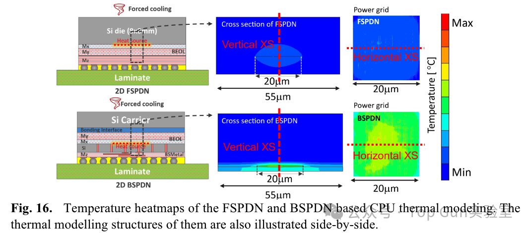 Cross-sectional temperature distribution:
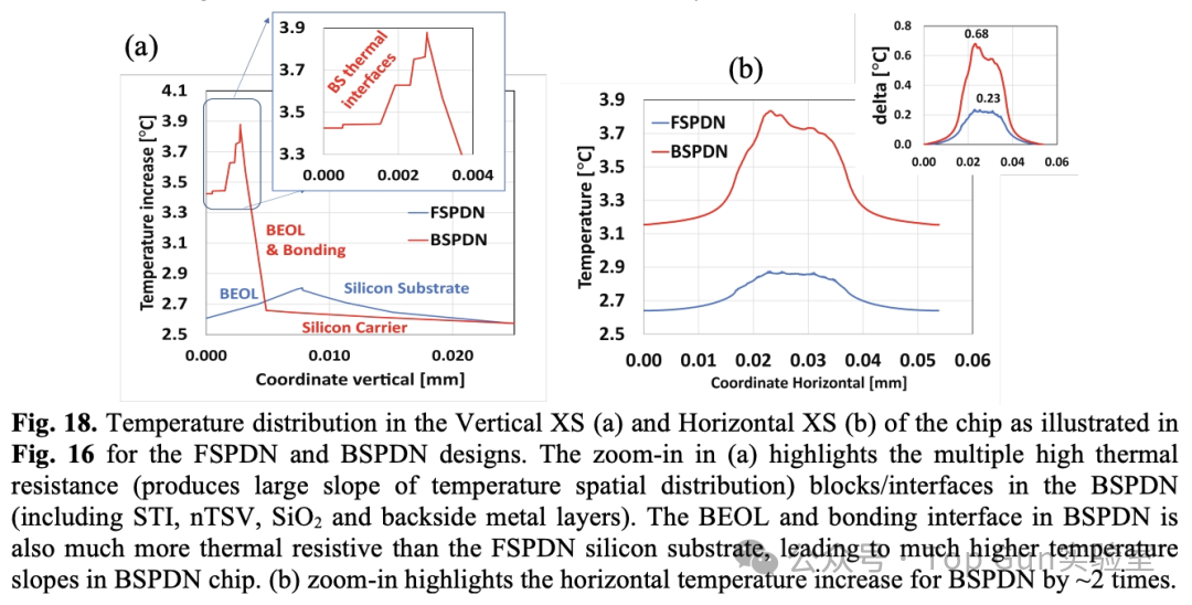 Thermal model of 3DIC:
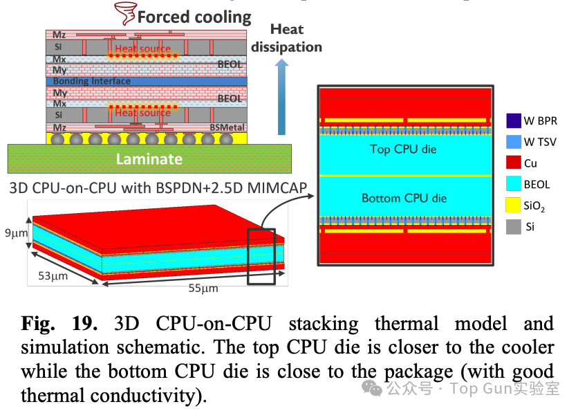 Temperature distribution of 3DIC:
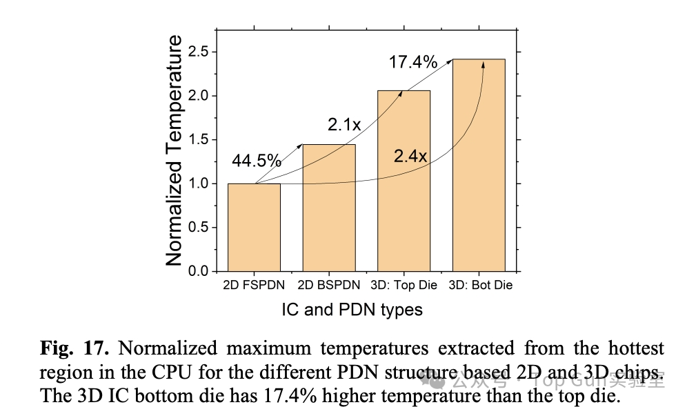
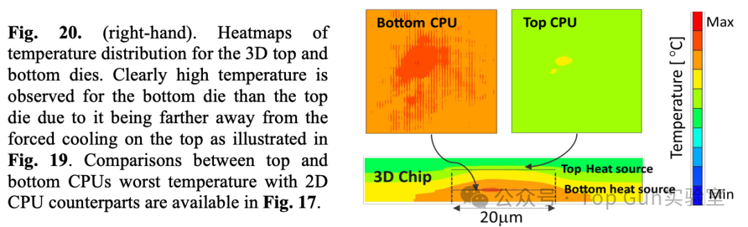
Temperature under different structures: 3D>2D BSPDN>2D FSPDN