
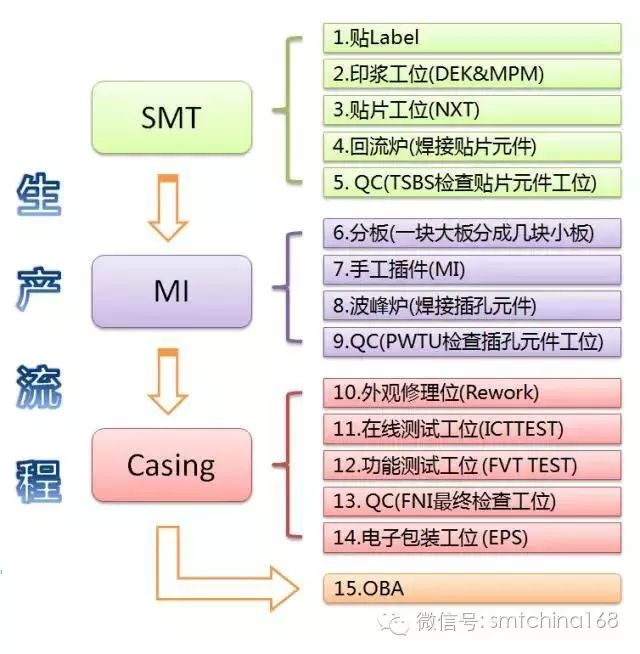
For employees in the electronics manufacturing industry, understanding the entire production process of PCBA in an electronic factory is not easy. Therefore, I have specially organized the main workstations on the DIP plug-in and SMT chip production lines into a flowchart, hoping everyone can clearly remember the different segments of the production line.

Analysis of SMT PCBA Soldering Quality Issues and Summary of Red Glue Printing Standards!

There are many reasons for voids in BGA solder joints, but the common ones are:
① Solder paste; different brands of solder paste contain varying amounts of flux and active ingredients. Excessive amounts of flux and active components generate gases that cannot completely evaporate in the constant temperature zone, leaving gas trapped in the solder joint, forming voids.
② Oxidation or contamination of the BGA solder balls or pads. In the reflow soldering constant temperature zone, when flux decomposes these oxides or contaminants, water vapor is formed that cannot be completely expelled, leaving voids in the solder joint.
③ Moisture in the BGA or PCB substrate can generate water vapor during high-temperature reflow soldering, leading to voids.
④ Temperature profile, especially if the constant temperature and time do not reach the optimal values according to the solder paste characteristics (consulting the solder paste supplier may help).
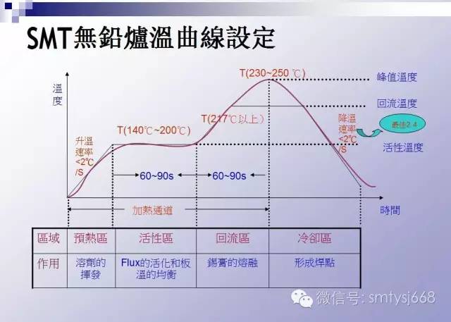
(Hot Air Reflow Oven Temperature Profile)

Another issue is the difference between voids inside BGA solder balls, voids on the PCB pad side, and voids at the chip end.
① Voids inside BGA balls are related to the incoming material. If voids appear in the BGA balls, you should take a few BGA parts and check with X-ray to see if the incoming material has issues.
② Voids inside BGA balls are also significantly related to moisture in the BGA substrate. You can try baking the BGA before placing it on the board.
③ Voids caused by solder paste can occur anywhere because gases can move within the molten solder.
④ Voids on the PCB pad side are related to oxidation of the PCB pads, moisture in the PCB, and vias and solder paste on the pads.
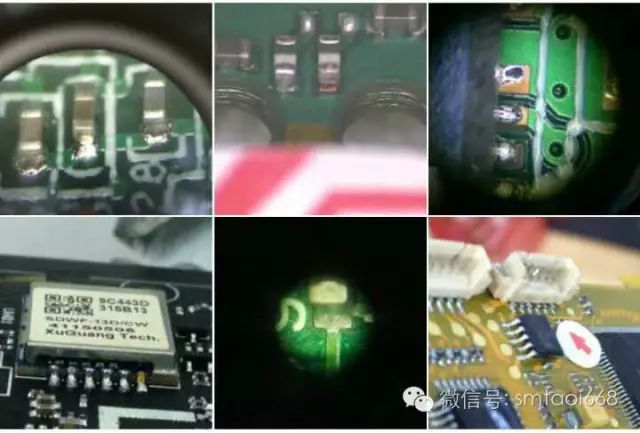
With the rapid development of the electronics industry, some large electronic processing companies have moved from the initial Pearl River Delta to the Yangtze River Delta, and now to the Beijing-Tianjin and Bohai Rim areas. SMT has become mainstream, transitioning from manual placement to automated equipment placement. Most use the SMT solder paste process, but many companies still have unavoidable through-hole component production (such as computer control, power supply products, etc.). This has led to the early red glue process and the later through-hole wave soldering process. However, the production of red glue processes has strict requirements for wave soldering control and PCB manufacturability design. Below, I will only introduce the design and process parameters of the red glue printing process, which are effective experiences gained from one year of experiments conducted at the company I currently work for, for reference in the SMT industry!
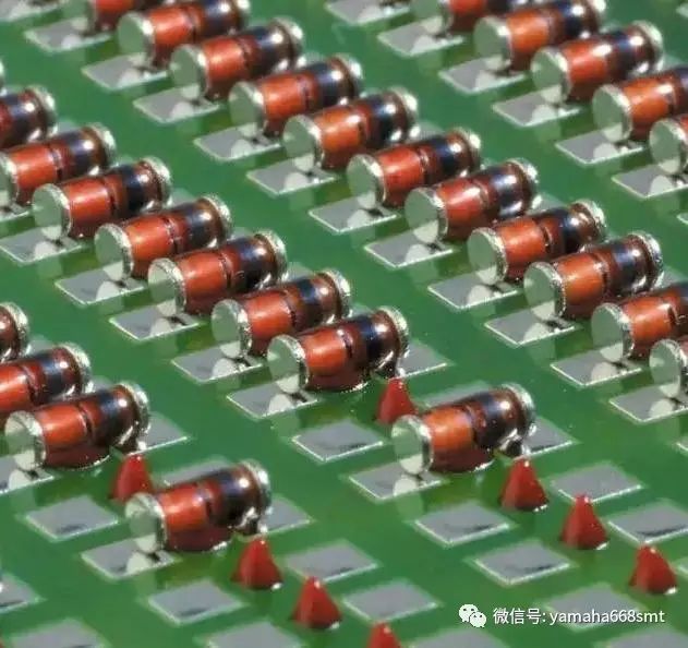
Selection and Use of Red Glue:
(1) Since it is not a dispensing process but a red glue printing process, there are certain requirements for the thixotropic index and viscosity of the red glue. If the thixotropic index and viscosity are poor, the printed shape will not be good, leading to collapse, which may cause some ICs not to adhere to the red glue and fall off. (Reference thixotropic index: 4-5; reference viscosity: (8-10)x1000000)
(2) Uncured glue on the circuit board can be wiped off with acetone or glycol ether or cleaned with a special red glue cleaner.
Understanding Glue: Red glue, also known as SMT adhesive or SMT red glue, is an adhesive in which hardeners, pigments, solvents, etc., are evenly distributed in a red paste, mainly used to fix components on printed circuit boards, generally applied through dispensing or stencil printing methods. After placing the components, they are heated in an oven or reflow soldering machine to cure. It is different from so-called solder paste; once heated and cured, it will not melt again, meaning the thermal curing process of the adhesive is irreversible. The effectiveness of SMT adhesive will vary depending on the thermal curing conditions, the connected items, the equipment used, and the operating environment. When using, one must choose the adhesive according to the production process.
Main components: base material (i.e., main polymer material), fillers, curing agents, and other additives.
Due to the influence of temperature on the viscosity, fluidity, and wetting characteristics of red glue, there are certain usage conditions and standardized management for red glue.
1. Red glue must have a specific flow number, numbered according to the quantity, date, and type of incoming materials.
2. Red glue should be stored in a refrigerator at 2~8℃ to prevent changes in characteristics due to temperature fluctuations.
3. Red glue must be brought to room temperature for 4 hours before use, following the first-in-first-out principle.
4. For dispensing operations, the red glue in the tube must be degassed. Any unused red glue should be returned to the refrigerator for storage, and old glue should not be mixed with new glue.
5. The temperature record sheet must be filled out accurately, noting the person who brought it to temperature and the time. The user must confirm that the temperature is okay before use.
Generally, expired red glue should not be used. It can be stored at room temperature for 7 days, at temperatures below 5℃ for more than 6 months, and at 5~25℃ for more than 30 days.
Equipment selection is based on process requirements and product-specific requirements:
Printing Method
The stencil hole size should be determined based on the type of component and the performance of the substrate, including thickness and hole size and shape. The advantages are speed and high efficiency.
Dispensing Method
Dispensing uses compressed air to apply red glue through a dedicated dispensing head onto the substrate. The size and amount of glue dots can be controlled by parameters such as time and pressure tube diameter. Dispensing machines have flexible functions. For different components, we can use different dispensing heads and set parameters to change the glue dots’ shape and amount to achieve the desired effect. The advantages are convenience, flexibility, and stability. The disadvantages include stringing and bubbles. We can adjust the operational parameters, speed, time, air pressure, and temperature to minimize these drawbacks.
Needle Turning Method
The needle turning method involves immersing a specially designed needle membrane in a shallow glue tray. Each needle tip has a glue dot; when the glue dot contacts the substrate, it will detach from the needle head, and the glue amount can vary based on the needle’s shape and diameter.
Allowed Ranges and Rejection Standards for SMT Red Glue Printing on Chip Materials and SOT Small Form Factor Transistors!
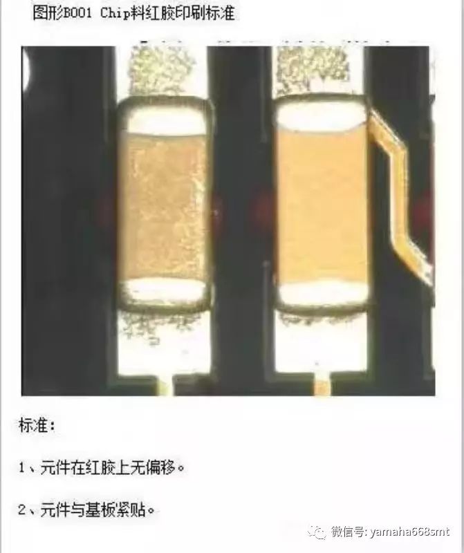
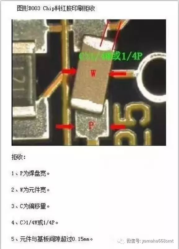
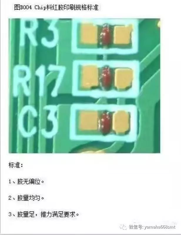
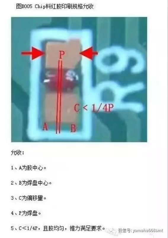
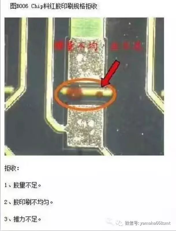
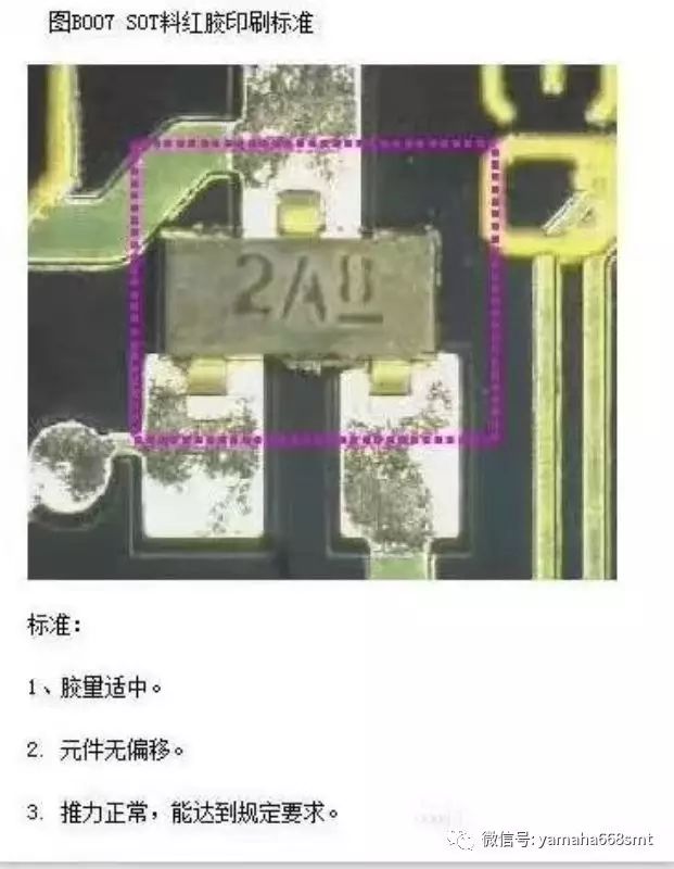
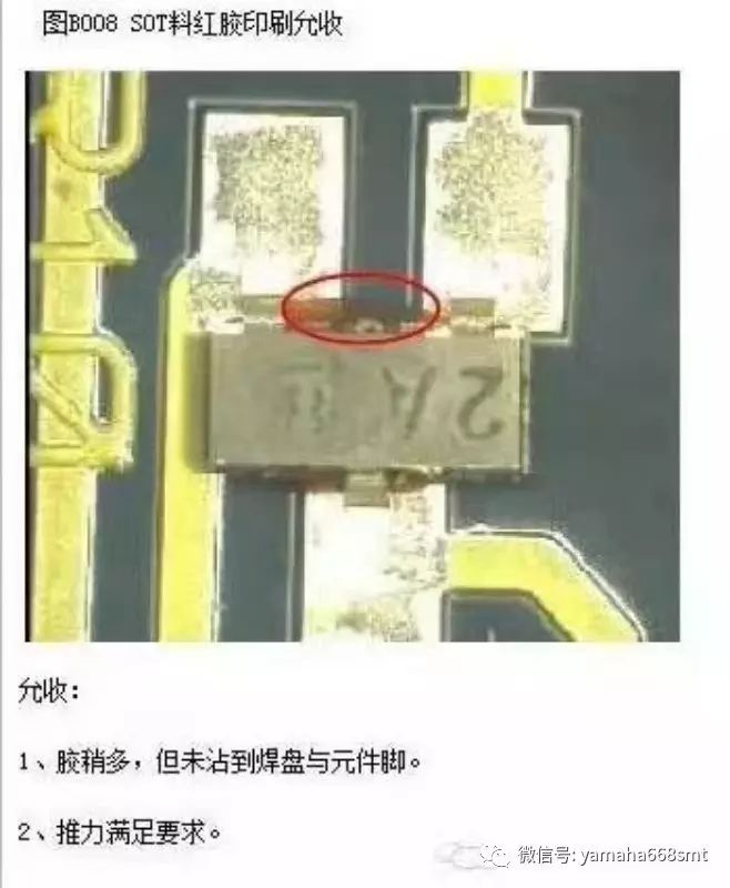
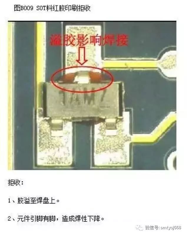
Allowed Ranges and Rejection Standards for SMT Red Glue Printing on Cylindrical and Square Materials!
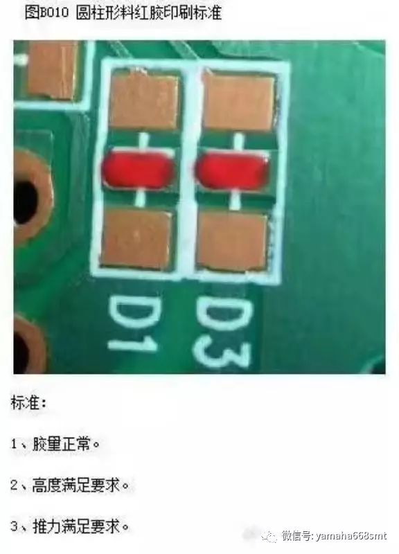
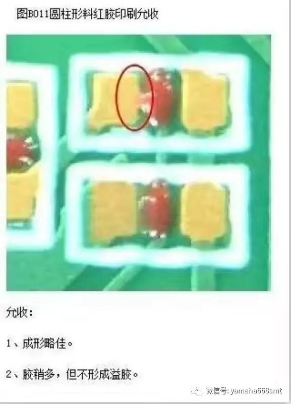
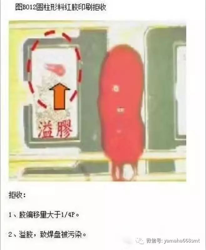
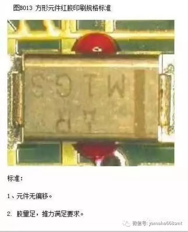
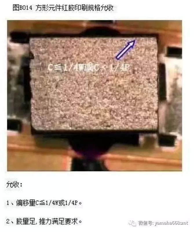
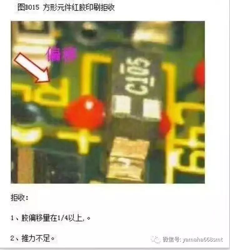
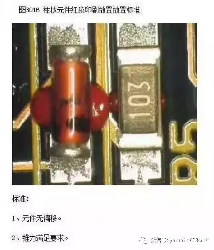
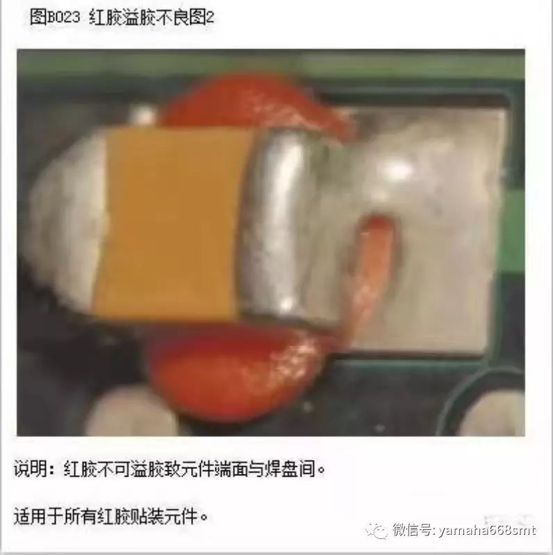
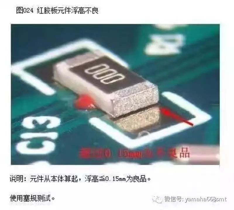
SMT PCBA Appearance Inspection Standards and Defect Analysis:
Inspection Environment:
1. Inspection environment: Temperature: 25+/-3℃, Humidity: 40-70%RH
2. Inspection of products should be carried out at a distance of 30cm from the inspector, within 1 meter of a 40W daylight lamp (or equivalent light source).
Sampling Level
QA sampling standard: Implement GB/T2828.1-2003 Level II normal inspection single sampling plan.
AQL values: CR:0 MAJ: 0.25 MIN:0.65
Inspection Equipment
Feeler gauge, magnifying glass, BOM list, placement position diagram
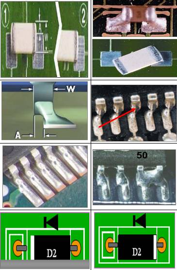
SMT Appearance Inspection Standards
Inspection Items:
1. Solder Balls: ● Solder balls violate minimum electrical spacing. ● Solder balls are not fixed within the no-clean residue or covered under conformal coating. ● The diameter of solder balls ≤0.13mm is acceptable; otherwise, it is rejected.
2. Cold Solder: ● The overlapping part (J) between the component solderable end and the PAD is clearly visible (acceptable). ● Insufficient overlap between the component end and the PAD (rejected).
3. Side Stand: ● The width (W) to height (H) ratio does not exceed 2:1 (acceptable). ● The width (W) to height (H) ratio exceeds 2:1 (see left image). ● The component solderable end is not fully wetted to the PAD surface. ● Components larger than 1206 class (rejected).
4. Upstanding: ● Chip components with lifted ends (upstanding) (rejected).
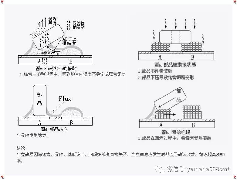
What Causes Upstanding?
Analyzing the mechanism of upstanding in chip components, the causes of upstanding need to be analyzed from the perspective of uneven wetting forces at both ends of the component. In actual production, many factors may lead to uneven wetting at both ends, but not all factors will necessarily cause upstanding. Let’s look at these factors:
-
Both soldering terminals of the component have poor solderability. If there is a difference in solderability between the two terminals, the wetting capability will differ, resulting in different wetting moments, which may lead to poor wetting, shift, or upstanding issues. If one end is not wetted at all, upstanding is almost guaranteed.
-
The volume difference in solder paste on the two pads may lead to different heat requirements for melting the solder paste, causing differences in melting rates and thus uneven wetting. However, this issue generally does not easily occur, as the stencil hole differences are usually not significant.
-
Offset in solder paste printing may lead to the solder paste not being fully deposited on the pads, which may prevent the component terminals from effectively contacting the solder paste, possibly resulting in no contact or minimal contact, which can easily lead to upstanding or shifting issues.
-
Differences in pad area are usually a design issue. It often happens that the design of the two pads is different, one end is NSMD pad design, and the other end is SMD pad design. This may relate to the electrical performance design of the product, such as power or ground pins. Such design differences may lead to two issues: one is that the different pad areas affect the flow of solder paste after melting on the pads, and the second is that the heat absorption and dissipation rates of the two pads differ, leading to temperature rise differences, which in turn cause differences in melting rates and wetting, thus potentially leading to shifting or upstanding issues.
-
The thickness of the solder mask, especially between the two pads, if the solder mask height is above the pad plane, during soldering, it acts like a seesaw, and even slight differences in wetting at both ends can be amplified, leading to poor wetting or upstanding effects.
-
Excessive spacing between pads can often be seen in many designs. If the spacing is large, the probability of upstanding is very high.
-
If there is solder paste beneath the component, it may elevate the component when melted, leading to issues similar to those caused by the solder mask.
-
Insufficient mounting pressure may prevent the component from effectively contacting the solder paste, which may lead to shifting during the transfer process, resulting in upstanding.
-
Issues with nitrogen usage. In today’s lead-free processes, nitrogen is sometimes used in reflow to ensure good soldering effects, which helps improve solderability or reduce voids. However, for the upstanding effect, if not controlled properly, it may backfire. The control of nitrogen mainly relates to the oxygen content; lower oxygen content is better. However, if the oxygen concentration is too high, due to the lack of oxygen hindrance, the solderability of the terminals increases, and the wetting of the solder also greatly improves, which may amplify the differences in solderability of the component terminals, leading to upstanding issues.
-
Insufficient placement accuracy can also lead to upstanding, which can be understood as being similar to the offset in solder paste printing. If solder paste cannot fully contact the two terminals of the component, differences in wetting may occur, leading to upstanding or shifting.
-
Profile issues. If the heating rate is too fast, it may cause the temperature on the board to rise or the heat distribution to be uneven, leading to upstanding.
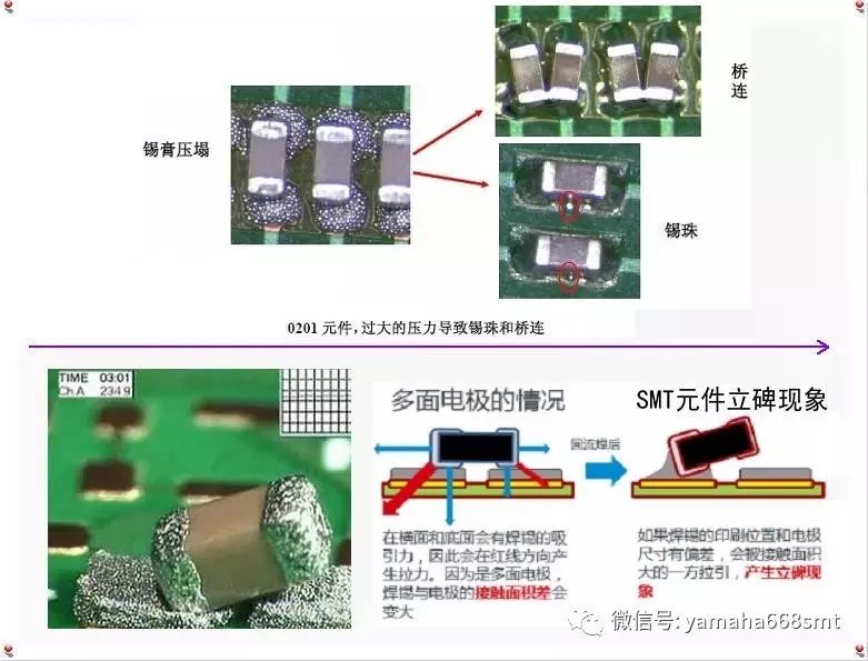
5. Flat, L-shaped, and wing-shaped lead offsets: ● Maximum side offset (A) should not exceed 50% of the lead width (W) or 0.5mm (0.02 inches) (acceptable). ● Maximum side offset (A) exceeds 50% of the lead width (W) or 0.5mm (0.02 inches) (rejected).
6. Side offsets on cylindrical end caps: ● Side offset (A) ≤ 25% of the component diameter width (W) or PAD width (P) (acceptable). ● Side offset (A) exceeds 25% of the component diameter width (W) or PAD width (P) (rejected).
7. Side offsets on rectangular or square solderable end components: ● Side offset (A) ≤ 50% of the component solderable end width (W) or PAD width (P) (acceptable). ● Side offset (A) exceeds 50% of the component solderable end width (W) or PAD width (P) (rejected).
8. J-shaped lead side offsets: ● Side offset (A) ≤ 50% of the lead width (W) (acceptable). ● Side offset (A) exceeds 50% of the lead width (W) (rejected).
Bridging: ● Component leads are soldered neatly to the PADs, without offset or short circuit phenomena (acceptable). ● Solder should not connect wires that should not be connected (rejected). ● Solder forming bridges between adjacent different wires or components (rejected).
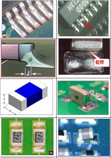
PCBA Appearance Inspection Standards
9. Reverse: ● The polarity mark (white silkscreen) on the component should match the silkscreen direction of the PCB diode (acceptable). ● The polarity mark (white silkscreen) on the component does not match the silkscreen on the PCB diode (rejected).
10. Excessive solder: ● The maximum height of the solder joint (E) can exceed the PAD or extend to the top of the solderable end cap metal coating but must not extend to the component body (acceptable). ● Solder has extended to the top of the component body (rejected).
11. Reverse White: ● Exposed conductive material of chip components facing away from the printed surface (acceptable). ● Each board is allowed only one ≤0402 component to be reverse white (acceptable). ● Exposed conductive material of chip components facing towards the printed surface (rejected). ● Each board is not allowed two or more ≤0402 components to be reverse white (rejected).
12. Cold solder: ● The solder joint between the component lead and the PAD should be well wetted and full, with no lifting of the component leads (acceptable). ● Misalignment of component leads (co-planarity) hinders the formation of acceptable solder (rejected).
13. Cold solder: ● During the reflow process, the solder paste fully extends, and the solder joint has a glossy surface (acceptable). ● The solder paste on the solder ball does not fully reflow, resulting in dark and irregular solder appearance, with unmelted solder powder (rejected).
14. Missing parts: ● The BOM list requires a component to be mounted at a specific placement position, but it is not mounted (rejected). Multiple parts: ● The BOM list requires a component to be mounted at a specific placement position, but it has been mounted (rejected); ● Extra components appear in places where they should not (rejected).
15. Damaged parts: ● Any edge peeling less than 25% of the component width (W) or component thickness (T) (acceptable). ● Maximum 50% loss of the metal coating at the end (each end) (acceptable). ● Any exposed cracks or notches; cracks, scratches, or any damage on glass components; any notches in resistive materials; any cracks or dents (rejected).
16. Blistering, delamination: ● The area of blistering and delamination does not exceed 25% of the spacing between plated through-holes or internal wires (acceptable). ● The area of blistering and delamination exceeds 25% of the spacing between plated through-holes or internal wires (rejected). ● The area of blistering and delamination reduces the spacing of conductive patterns to violate minimum electrical spacing (rejected).
Sponsor Advertisement
KeTu Technology Co., Ltd.
Quickly follow this public account to learn more!

Disclaimer: The copyright of the articles, images, audio, video files, and other materials reproduced by this public account belongs to the copyright owner. The purpose of reproduction is to convey more information. If the original author believes that their work is not suitable for public viewing or should not be used without compensation, please contact us promptly to take swift action to avoid unnecessary losses for both parties.
Original Statement: The content is not original; originality is limited to the combination and filtering of forms!
Feel free to share in your circle of friends, forwarding is support! You can express your views on this article by clicking “Write a Message” at the bottom!