
1. Introduction
The copper in the vias of a printed circuit board (PCB) is akin to the neural network (blood vessels) of the human body, interspersed within the substrate “body” to provide the basic pathways for signal transmission and current conduction. Once a via copper break occurs, it is like a nerve being severed, preventing signal commands from being transmitted or causing circuit links to fail, leading to complete product failure.
Via copper breakage is caused by the insufficient tensile strength of the via copper to withstand the thermal stress induced by substrate expansion. There are many reasons for the decrease in tensile strength of the via copper: such as the “twin crystal” defect in the copper plating [1], pinhole defects in the copper plating [2], insufficient copper thickness, and via breakage etc. Some causes are relatively easy to identify, such as twin crystal and pinhole defects, which can be recognized by magnifying observations after specific etching treatments. However, some causes of via copper breakage failures can be confusing, such as via breakage, which may be due to etching process bite, or residual etching solution after the solder mask process [3], or bite during surface treatment processes. Via copper breakage typically only becomes apparent after the PCB product has been shipped and is in the assembly or usage phase, making its failure somewhat hidden. Determining at what stage the via copper was bitten to form the break requires a certain level of on-site experience.
In the actual analysis and guidance of PCB factories for quality improvement, it has been found that some process engineers have insufficient understanding of the failure causes, leading to misattribution of the reasons. This article analyzes three cases of via breakage failures, providing a detailed comparison of their failure characteristics and causes, offering references for PCB companies in the industry to identify the causes of via breakage failures, delineate responsibilities, and carry out corrective actions.
2. Case Analysis
1. Corrosive Via Breakage Failure
1.1 Analysis Process
A certain product exhibited screen flickering and black screen phenomena during end-use, and after slicing the PCBA, via breakage was discovered. After determining the open circuit failure of the via through electrical testing, a slice analysis was performed, revealing that the via structure was a solder mask semi-plugged via. The copper breakage was located at the edge of the solder mask plug. Upon magnified observation of the break morphology, a “crescent” shaped copper loss phenomenon was observed at the break, with some edges showing copper corrosion and blackening. See Figure 1.
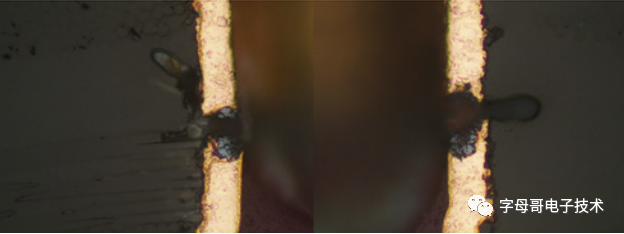
Figure 1: PCBA Failure Via Slice Image
To verify whether the copper corrosion in the via was introduced during the SMT process or was due to the PCB itself, a slice analysis of the same batch of PCB blank was conducted, as shown in Figure 2, revealing that copper corrosion and blackening also existed in the via, indicating that the copper layer had been corroded and discolored during the PCB manufacturing process, rather than due to corrosive substances (such as flux, cleaning agents, etc.) during the SMT process. The corroded and blackened copper in the via was observed under SEM, revealing a very loose copper layer structure, as shown in Figure 3.
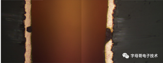
Figure 2: PCB Blank Via Slice Image
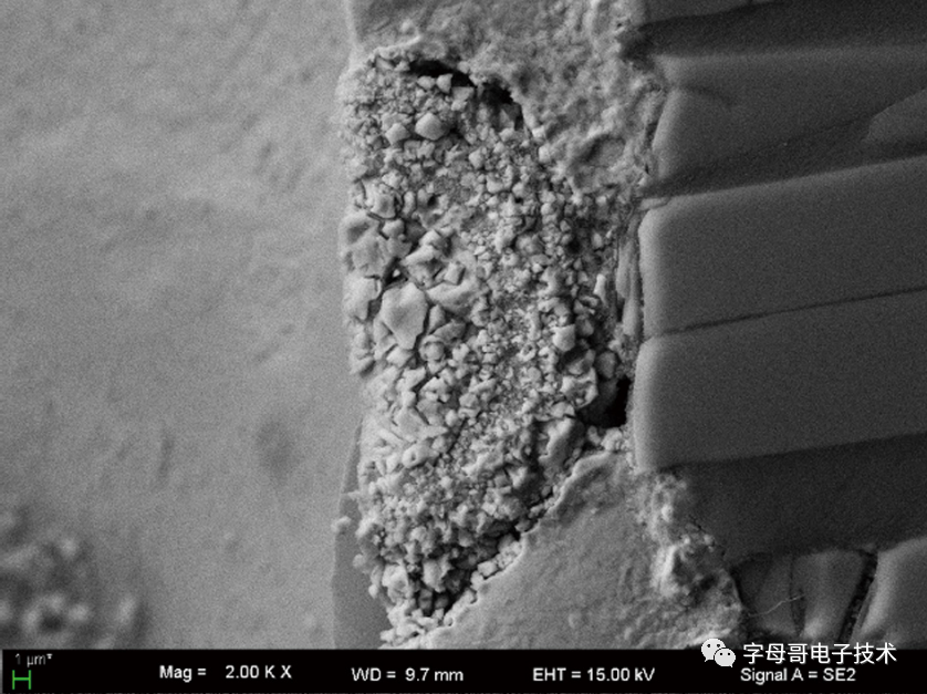
Figure 3: SEM Image of Corroded and Blackened Copper Location
1.2 Comprehensive Analysis
From the slice results of the failed sample, the failure manifested as complete breakage of the via copper. The break exhibited a “crescent” shaped copper loss phenomenon, which could easily be misjudged as being caused by insufficient protection of the via copper leading to etching. However, careful observation revealed that the edges of the break exhibited copper corrosion and blackening, and a slice of the same batch of PCB blank revealed similar conditions on the blank, allowing us to rule out the factors of the SMT process, indicating that the copper had been corroded after the PCB was manufactured and before SMT. After corrosion, the copper not only underwent compositional changes (pure copper transformed into copper compounds) but also significant structural changes, where normally, the copper grains are tightly bonded, but after corrosion, the copper compounds exhibit a loose morphology, which deteriorates the tensile strength of the via copper, severely reducing its tensile strength, making it unable to withstand the expansion stress of the substrate during subsequent SMT processes, leading to via copper breakage failure. The via structure is a solder mask semi-plugged via, making liquid exchange within the via difficult, and it is even possible that due to surface tension, air within the via is not easily expelled, increasing the difficulty of cleaning the process chemicals within the via, as shown in Figure 4. These inadequately cleaned vias can lead to chemical residues, providing a medium for the corrosion of the via copper during subsequent PCB storage.

Figure 4: Schematic of Liquid Flow in Solder Mask Semi-Plugged Via
1.3 Summary
Corrosive via breakage mostly occurs in solder mask semi-plugged or solder mask plugged vias, with the failure location exhibiting a “crescent” morphology, generally accompanied by the presence of blackened copper.
2. Etching Via Breakage Failure
2.1 Analysis Process
The sample shown in Figure 5 is a standard leaded tin-spray PCB, which exhibited non-conductive vias during aging tests at the client site after SMT production.
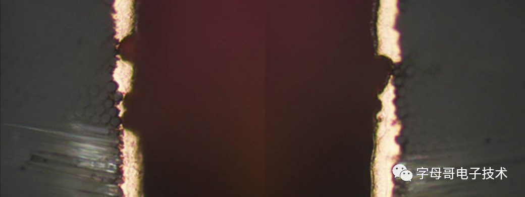
Figure 5: Representative Image of Failed Via Slice
The slice clearly shows a significant via breakage phenomenon, with the break exhibiting a “crescent” morphology, the break area being relatively clean, and no corrosion or blackening observed at the edges. The copper thickness at the break is very thin, with even instances of disconnection. Observations under SEM revealed that the morphology of the break was irregular and the shape was not uniform, as shown in Figure 6.
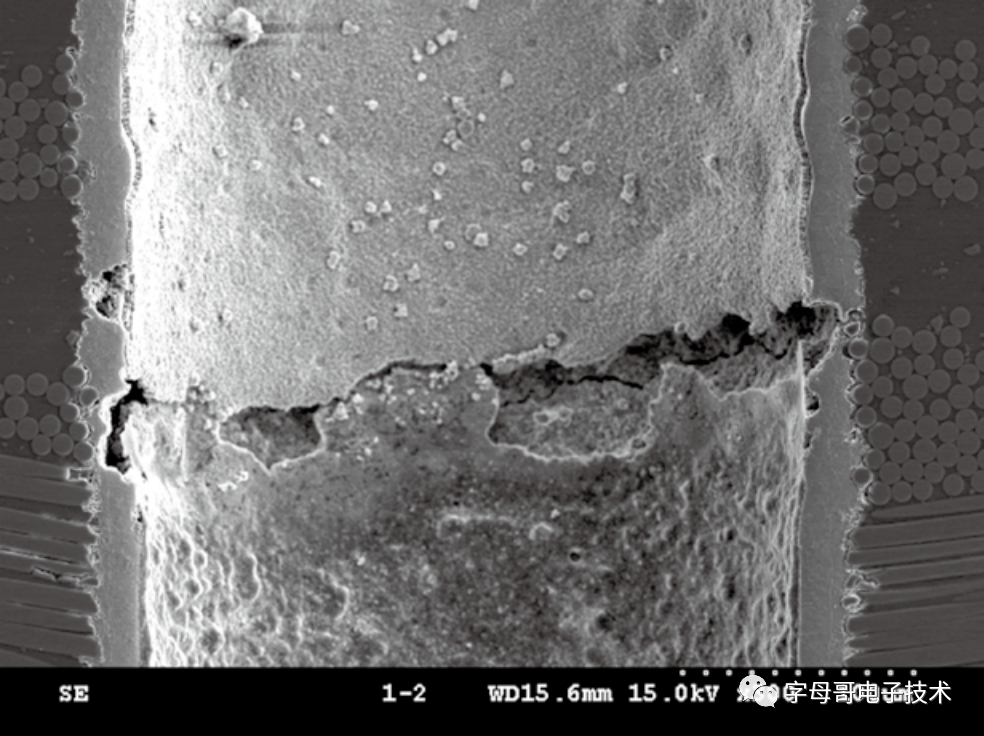
Figure 6: Representative SEM Image of Failed Via
2.2 Comprehensive Analysis
Considering the PCB manufacturing process of this board, after copper plating, a tin plating layer is required as a corrosion-resistant layer before stripping and etching the circuit. When the tin plating layer is defective, it leads to insufficient protection during the etching process, causing the via copper to be eroded by the etching solution, resulting in the via breakage phenomenon.
2.3 Summary
Etching via breakage also exhibits a “crescent” morphology, but unlike corrosive via breakage, this type of failure phenomenon is relatively clean at the break, with no loose copper morphology.
3. Galvanic Effect Via Breakage Failure
3.1 Analysis Process
A certain tin-plated board failed the functional test after reflow soldering, and after investigation, it was determined that the failure was caused by via breakage in the PCB.
Multiple via locations on the PCB were sliced for analysis, as shown in Figure 7. Most of the via breakages exhibited a “crescent” shape, while around the severely broken vias, the tin layer was significantly thicker than normal levels, and at lightly broken vias, the tin layer was suspended above the copper surface. The suspended phenomenon indicates that there was a copper layer present as a support for the deposition layer during the initial tinning, suggesting that the breakage did not occur before the tinning process, but rather formed during the tinning process. Based on the failure characteristics of the thick tin layer surrounding the severely broken areas, it can be concluded that a significant “Galvanic” reaction occurred during the tinning process.
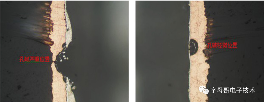
Figure 7: Representative Slice Image of Failure Location
3.2 Comprehensive Analysis
The Galvanic effect refers to the electrochemical reaction that occurs between two metals due to potential differences. In most cases, the Galvanic effect typically occurs at the junction of wires and solder masks, with the main mechanism illustrated in Figure 8. Under normal circumstances, during the tinning process, the Cu substrate continuously loses electrons to form Cu+, while Sn2+ ions in the solution continuously gain electrons and deposit on the Cu substrate surface. When the copper substrate is completely covered, the reaction tends to stop. However, when there are small cracks such as solder mask undercuts on the surface of the circuit, the exchange of chemicals within the cracks is insufficient, failing to provide enough Sn2+ ions, while other components in the solution still promote the conversion of Cu to Cu+ ions, which continue to dissolve in the solution. Excess electrons are captured by Sn2+ in the tinning solution, leading to continued deposition on the surface. Therefore, the locations where the Galvanic effect occurs generally have relatively thick chemical plating layers. The Galvanic effect is not only likely to occur during the chemical tinning process but is also common in chemical silver plating processes.
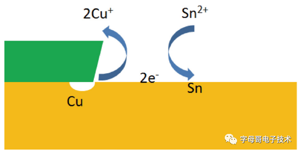
Figure 8: Mechanism Diagram of Galvanic Effect in Tinning Surface Treatment
Because the Galvanic effect mostly occurs on the surface of wires, many people often overlook that the conditions for the Galvanic effect can also occur within the via copper. For example, solder mask limited via pads (Figure 9, position 1), developer residues remaining in the via (Figure 9, position 2), or poor bonding between solder mask semi-plugged vias and via walls (Figure 9, position 3), all create narrow gaps that provide favorable conditions for the chemical deposition plating process to induce the Galvanic effect.
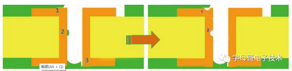
Figure 9: Schematic of Galvanic Effect Occurring in Via Copper
3.3 Summary
The Galvanic effect via breakage generally occurs in vias during tinning or silver plating processes. Although it also exhibits a “crescent” morphology and the break area is relatively clean, it is very similar to etching-type via breakage, but the surrounding area generally exhibits an abnormal thickening of the plating layer. The presence of suspended plating at lightly broken areas is an important piece of evidence distinguishing it from etching-type via breakage and is a significant characteristic of Galvanic effect via breakage.
3. Conclusion
This article introduces three types of via copper breakage failures caused by via breakage, which superficially appear similar, all exhibiting a “crescent” morphology, leading to some interference. However, upon careful differentiation, the three have essential differences: corrosive via breakage is accompanied by loose copper morphology and blackened copper; etching-type via breakage has relatively clean edges with no loose copper or blackened copper; and Galvanic effect via breakage is accompanied by abnormal thickening of the plating layer. By distinguishing the morphology on the slice cross-section and aided by SEM magnified observations, it is not difficult to confirm the true cause of the failure, thus finding the “right prescription” to solve the problem.
References:[1] Luo Bin. Research on Columnar Crystallization of Electroplated Copper Layer in PCB Holes [D]. Harbin Institute of Technology, 2009.[2] Peng Hualing. Research on Low Porosity HEDP Copper Plating Process and Coating Performance [D]. Nanchang Hangkong University, 2017.[3] Wang Zhao. A Method to Replace Aluminum Sheet Plugging [C]. Printed Circuit Information 2016(11), 64~66.[4] Du Sen. Experimental Research on Side Etching Defects in Silver Plating Process [J]. Printed Circuit Information 2012(8), 40~46

Some screenshots from electronic books
【Complete Set of Hardware Learning Materials Collection】