|
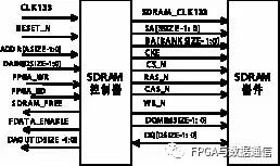
Introduction — In FPGA-based image acquisition and display systems, large-capacity and high-speed memory is often required. Among various random access memory devices, SDRAM is an ideal choice due to its low cost, small size, high speed, and large capacity. However, the control logic of SDRAM is quite complex, and the timing requirements are very strict, making it inconvenient to use. This necessitates a dedicated controller that allows system users to easily operate SDRAM. Therefore, this article proposes a design method for an FPGA-based SDRAM controller, implemented in Verilog. Simulation results show that the controller designed using this method can form an SDRAM interface as shown in Figure 1 within the FPGA chip, making it very convenient for system users to operate SDRAM. Overview of SDRAM — The pins of SDRAM devices are divided into three categories: control signals, addresses, and data. Typically, an SDRAM contains several BANKs, and the storage units of each BANK are addressed by rows and columns. Due to this special storage structure, SDRAM has the following operational characteristics. ● Initialization of SDRAM — After powering on for 100 to 200 μs, SDRAM must be configured through an initialization process to set the mode register, the value of which determines the operational mode of SDRAM. ● Accessing storage units — To reduce the number of I/O pins, SDRAM multiplexes address lines. Therefore, when reading from or writing to SDRAM, the ACTIVE command is first used to activate the BANK to be read or written, and the row address is latched. Then, when the read or write command is valid, the column address is latched. Once a BANK is activated, it can only be reactivated after executing a precharge command. ● Refreshing and precharging — The storage units of SDRAM can be understood as capacitors that tend to discharge, so a timed refresh cycle is necessary to prevent data loss. The refresh cycle can be calculated as (minimum refresh cycle ÷ clock cycle). Precharging or closing an activated BANK can be done for a specific BANK or simultaneously for all BANKs, with A10, BA0, and BA1 used to select the BANK. ● Operational control — The specific control commands for SDRAM are assisted by some dedicated control pins and address lines. The states of CS, RAS, CAS, and WR at the rising edge of the clock determine the specific operational actions, while the address lines and BANK selection control lines serve as auxiliary parameters in some operational actions. Due to the special storage structure, there are many operational commands for SDRAM, unlike SRAM, which only has simple read and write commands. Design and Implementation of the SDRAM Controller ● Overall design block diagram and external interface signals
Figure 1 — The schematic diagram of the SDRAM controller and its external interface signals is shown in Figure 1. The interface signals on the right side of the controller are directly connected to the corresponding pins of the SDRAM, which will not be discussed here. The interface signals on the left side of the controller are the system control interface signals connected to the FPGA, where CLK133 is the system clock signal, RESET_N is the reset signal, ADDR is the SDRAM address signal provided by the system, DAIN is the data signal used by the system to write to SDRAM, FPGA_RD and FPGA_WR are the system read and write request signals (1 is valid, 0 is invalid), SDRAM_FREE is the idle state indicator signal for SDRAM (0 is idle, 1 is busy), and FDATA_ENABLE is the data transmission indication signal from the controller to the system (when 0, data transmission to SDRAM is not possible; when 1, if it is a system read operation, the system can receive data from SDRAM through DAOUT, and if it is a write operation, the system can send data to SDRAM through DAIN).
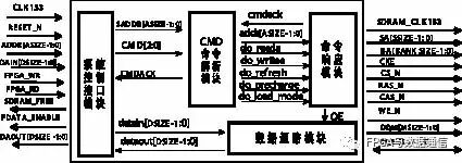
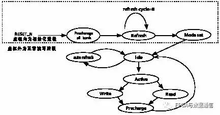
Figure 2 — The structure of the SDRAM controller is shown in Figure 2, which includes four modules: the system control interface module, CMD command parsing module, command response module, and data path module. The system control interface module is responsible for receiving system control signals and generating different CMD command combinations; the CMD command parsing module receives CMD commands and decodes them into operational instructions; the command response module receives operational instructions and generates the operational actions for SDRAM; the data path module controls the effective input and output of data. — The implementation principle of the state machine for the SDRAM controller design is shown in Figure 3, which includes 9 states. The states from Precharge to Mode set represent the initialization process after powering on SDRAM, while the remaining states represent the normal read, write, and refresh operations of SDRAM.
Figure 3 ● Design of Each Module — (1) System Control Interface Module — This module contains the initialization mechanism and system instruction analysis mechanism. The initialization mechanism not only completes the initialization configuration of SDRAM but also configures the controller to ensure that its operational mode is consistent with that of the external SDRAM. The process is as follows: controlled by a counter, after approximately 200 μs of system power-on, the SDRAM initialization configuration is first performed using a Precharge all bank command to precharge all BANKs, followed by multiple Refresh commands, and then the mode configuration command LOAD_MODE to set the operational mode of SDRAM. After that, the controller’s initialization configuration is performed, first issuing the LOAD_REG1 command to load the mode word into the controller, followed by the LOAD_REG2 command to load the refresh counter value into the controller, completing the controller’s initialization configuration. — After the above initialization process is completed, the system instruction analysis mechanism can receive and analyze the system’s read and write signals and address information, as well as the CMDACK signal fed back from the next module, generating corresponding CMD commands and SADDR address information for the CMD command parsing module. Through program settings, it is possible to determine when to issue Precharge or Refresh CMD commands based on the parameters configured during initialization, thereby simplifying system control. Whenever CMDACK is received as 1, it indicates that the CMD command has been issued and is valid, at which point a NOP command (CMD=000) must be issued. It should be noted that SADDR is time-multiplexed; during the initialization loading mode, SADDR is used to transmit user-defined mode word content; during normal read and write periods, SADDR serves as the address line to transmit the row, column, and block addresses required by SDRAM. Additionally, the system instruction analysis mechanism will provide feedback on the state of the SDRAM operation to the system user through the SDRAM_FREE and FDATA_ENABLE signals. Detailed CMD command descriptions can be found in Table 1. — (2) CMD Command Parsing Module — This module judges the CMD commands, and the result is to output the corresponding operational instruction signals to the command response module. For example, when CMD is 001, it will output the do_read signal as 1; when CMD is 010, it will output the do_write signal as 1. At any given time, only one valid operational instruction will be output. — — In addition, this module contains mode registers used to preset certain mode parameters, mainly including three types: the first type is the SDRAM mode control register, which sends its value to the SDRAM mode register during the LOAD_MODE command to control the operational mode of SDRAM. The second type is the parameter register of the SDRAM controller (LOAD_REG1), which ensures that the operational mode of the SDRAM controller matches that of the external SDRAM device. The third type is the refresh cycle control register of SDRAM, which presets the user-defined automatic refresh count value for the SDRAM refresh cycle. The preset values of these three types of registers are transmitted to the system control interface module during initialization via SADDR. — (3) Command Response Module — The function of this module is to perform operational actions that comply with SDRAM read and write specifications based on the operational instructions obtained from the CMD command parsing module, to carry out the desired operations; it provides the data selection signal OE to control the data path module (OE is 1 during write operations and 0 during read operations). Additionally, this module processes the system’s non-multiplexed address ADDR into the multiplexed address for SDRAM, sending it to SA and BA in a time-multiplexed manner. The address multiplexing method in the program is as follows: — assign raddr = ADDR[ROWSTART + ROWSIZE -1:ROWSTART] // raddr is the row address — assign caddr = ADDR[COLSTART + COLSIZE -1:COLSTART] // caddr is the column address — assign baddr= ADDR[BANKSTART + `BANKSIZE -1:BANKSTART] // baddr is the BANK address — (ROWSTART, COLSTART, BANKSTART are the starting bits of row, column, and block in ADDR) — In the program, the CMD instructions for WRITEA and READA implicitly include the ACTIVE command, so after receiving the do_write or do_read instruction, this module will first perform the activation action, and after the CAS delay time specified in the initialization configuration, it will proceed with the read or write action. For example, during initialization, if the mode word specifies CAS=2 and BURST LENGTH=PAGE, upon receiving do_write=1 from the command interface module, it will first perform the activation action and provide the row address (issuing RAS_N=0, CAS_N=1, WE_N=1, SA=raddr), and after a delay of 2 clock cycles, it will perform the write action and provide the column address (issuing RAS_N=1, CAS_N=0, WE_N=0, SA=caddr). — Furthermore, after receiving various operational instructions, this module will feedback the cmdack signal as 1 to the CMD command parsing module, and ultimately feedback the CMDACK signal as 1 to the system control interface module. If no operational instructions are received, cmdack=0 and CMDACK signal will be 0. — Usage of the Controller and Simulation Timing — Depending on the different read and write requirements of the system design for SDRAM, simple parameter modifications to the controller (mainly the settings of the mode word during initialization) can make the control of SDRAM meet specific requirements. This controller simplifies the operation of SDRAM for the system. For example, in a write operation, after initialization, as long as SDRAM is idle, the system will receive a valid SDRAM_FREE signal, at which point it can issue the FPGA_WR instruction while providing the ADDR address information. Upon receiving a valid FDATA_ENABLE feedback, the system will write data through DAIN to SDRAM, thus completing the write operation without needing to concern itself with SDRAM’s refresh and precharge. |