
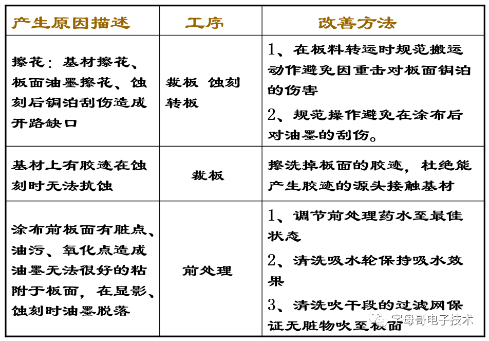
1. PCB Inner Layer Defects – Open Circuits, Notches, Pinholes
1. Common Defects (Open Circuits, Notches, Pinholes) Image Description
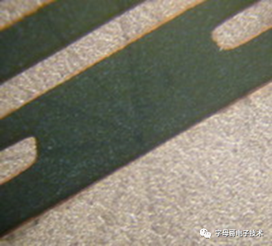
1.1. Open Circuit due to Ink Peeling (caused by poor surface treatment affecting ink adhesion)
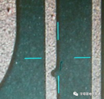
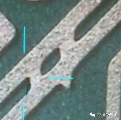
1.2. Notch in the Circuit (Pinholes on the Ink Surface after Coating)
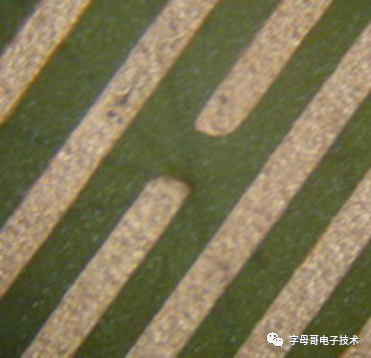
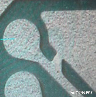
1.3. Open Circuit (Debris on the Film Positioning)
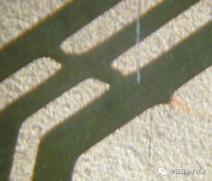
1.4. Smearing (Ink Smudging)
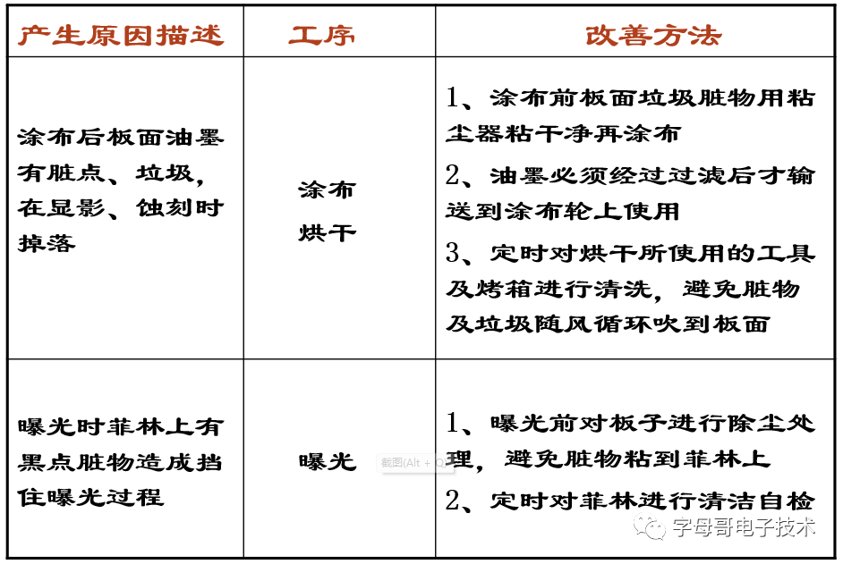
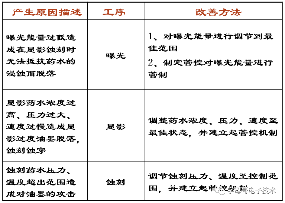
2. Analysis and Improvement of Common Defects (Open Circuits, Notches, Pinholes)
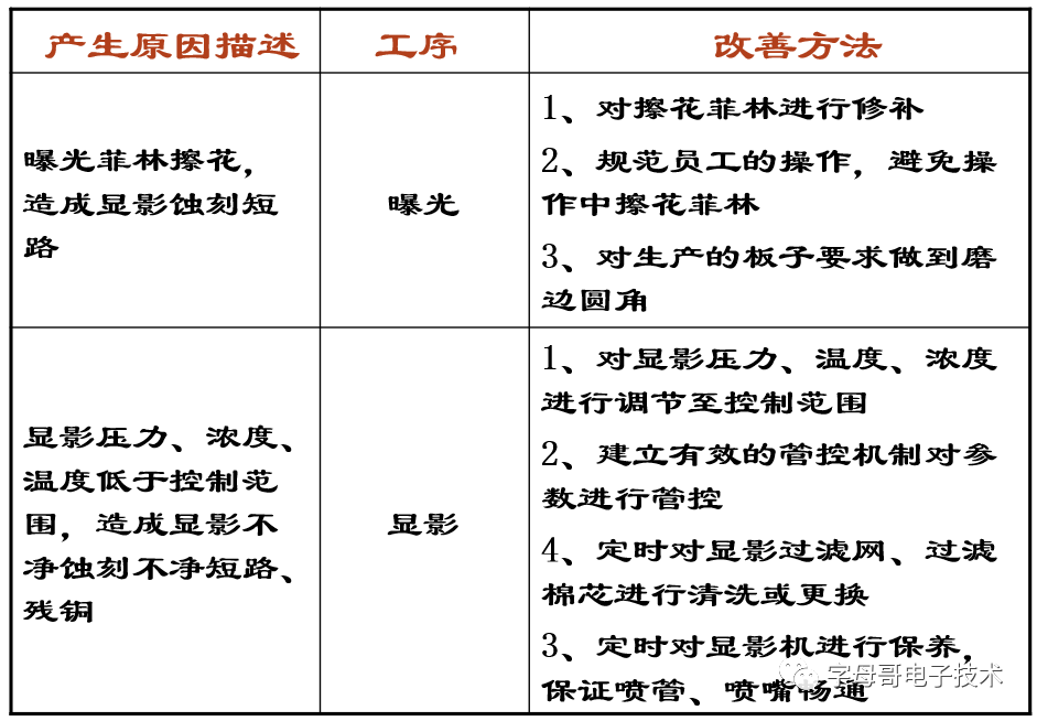
2. PCB Inner Layer Defects – Short Circuits, Residual Copper
-
Common Defects (Short Circuits, Residual Copper) Image Description
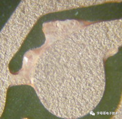
1.1. Foreign Object Short Circuit (Filamentous Foreign Object under Ink)
1.2. Short Circuit (Film Smudging Positioning Short Circuit)
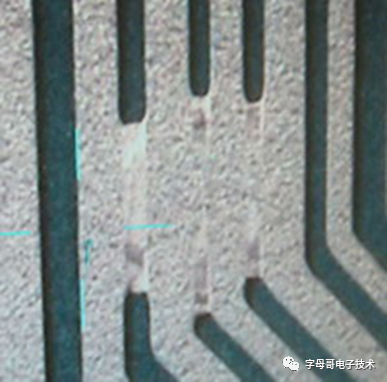
1.3. Residual Copper (Glue Marks or Poor Material)
1.4. Short Circuit (Ink Adhesion Not Clean)
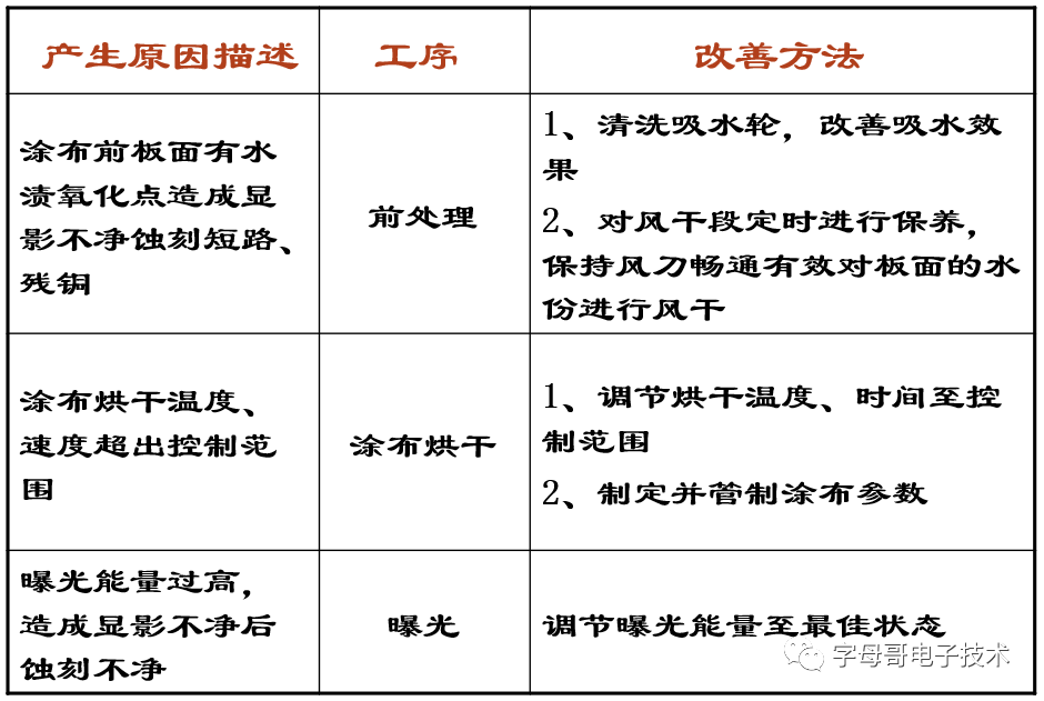
2. Analysis and Improvement of Common Defects (Short Circuits, Residual Copper)

Some Screenshots from Electronic Books

【Complete Set of Hardware Learning Materials Collection】