1. Research Background and Objectives
- Current Status and Challenges Traditional polymer surface selective metallization methods are costly, complex, and often use toxic chemicals (such as chromic acid), which are harmful to the environment and health. Existing technologies (such as laser direct writing and conductive inkjet printing) require customized equipment or special materials, limiting rapid prototyping development.
- Objective To develop a low-cost, environmentally friendly, and easy-to-implement process for rapid electronic function integration of 3D printed polymer parts, promoting the development of miniaturized electronic devices (such as sensors, wireless transmission coils, and flexible circuits).
2. Core Process: Rapid 3D-Plastronics
1. Process Steps
- 3D Printing Use vat photopolymerization technology to print 3D polymer parts with grooves (defining electronic circuit paths). Materials can be high-temperature resistant resins (for high-temperature scenarios) or flexible resins (for bendable devices).
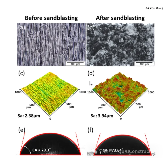
- Surface Treatment Increase surface roughness (from 2.38 µm to 3.94 µm) and wettability (contact angle from 79.3° to 73.64°) through sandblasting, enhancing the adhesion of the metal-polymer interface, replacing traditional toxic chemical etching.
- Selective Metallization
- Immerse in colloidal palladium catalyst solution to ensure uniform adhesion of the catalyst to the surface;
- Remove the catalyst from non-groove areas by manual polishing, retaining the catalyst only in the grooves;
- Use electroless copper plating to form conductive copper lines within the grooves, with a thickness of 5-50 µm and a resistivity as low as 2.25 µΩ・cm (close to 74% conductivity of bulk copper).
2. Key Advantages
- Environmentally Friendly and Low Cost No need for lasers, multi-material printers, or toxic chemicals; only standard photopolymer resins and sandblasting treatment are used.
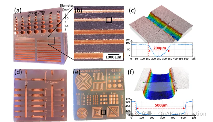
- High Selectivity and Precision Capable of manufacturing lines as narrow as 200 µm and vias up to 36 mm deep, suitable for complex 3D structures (such as curved surfaces and multilayer circuits).
- Strong Adhesion and Stability The adhesion of the copper layer is verified by the Scotch Tape Test and pull-off tests, with a tensile strength of 10.1 N/mm². After 50,000 cycles in bending tests, the resistance only increased by 8%.
3. Performance Verification and Results
- Surface Characteristics After sandblasting, the surface roughness increased, and hydrophilicity improved. The copper layer on samples without sandblasting easily detached, while sandblasted samples exhibited a uniform and dense copper plating.
- Electrical Performance The resistivity of the electroless copper lines is 2.25 µΩ・cm, which can be further reduced after plating, meeting the needs of low-power circuits; heating resistors can reach 150°C at 7.3 W power, with a stable temperature coefficient of resistance (0.00327/°C), suitable for temperature sensing.
- Compatibility with Complex Structures Successfully manufactured hemispherical wireless power transmission coils with a quality factor (Q) of 250 (at 6.78 MHz), outperforming planar coils, validating the feasibility of curved electronic integration.
- Flexible Electronics Performance Copper lines on flexible resin substrates maintained stability after 50,000 cycles at a 10 mm bending radius, with resistance changes of less than 10%, suitable for wearable devices.
4. Application Scenarios
- High-Temperature Devices Heating elements and temperature sensors made from high-temperature resistant resins, suitable for industrial temperature control scenarios.
- Wireless Power Transmission Hemispherical copper coils achieve efficient electromagnetic induction, with quality factors superior to traditional planar designs, applicable for three-dimensional wireless charging of IoT devices.
- Flexible Electronics Microcontroller circuits on flexible substrates (such as gaming dice and capacitive buttons) demonstrate the potential of bendable electronic devices.
- Complex 3D Circuits Integration of multilayer lines and vias in a cubic model validates the capability of high-density electronic functions in three-dimensional space.
5. Conclusion and Outlook
- Innovation The first combination of sandblasting treatment with electroless copper achieves environmentally friendly, low-cost 3D electronic integration, breaking the dependence of traditional technologies on equipment and materials.
- Limitations Currently, the minimum line width is limited by the 3D printing resolution (200 µm), and the uniformity of metallization for deep vias (>36 mm) needs improvement.
- Future Directions Expand to high-performance polymer and ceramic substrates, explore automated sandblasting and metallization processes, and promote applications in aerospace, biomedical, and other fields.